blogs
Qtech Technology Co., Ltd
SMT / DIP / PCB assembly /
Testing / BGA reworking
QUOTE
close
SMT / DIP / PCB assembly /
Testing / BGA reworking

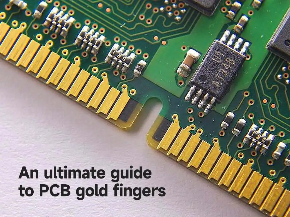
PCB gold fingers are a row of square pads on a PCB’s edge that have been hard gold plated for electrical conductivity. PCB gold fingers, often known as “edge connectors,” are a standard component in many electronic devices.
This article thoroughly explains printed circuit board (PCB) gold fingers, including topics like PCB gold finger width and kinds, the hard gold plating technique, and PCB gold finger notches. In this article, we shall discuss PCB gold fingers.
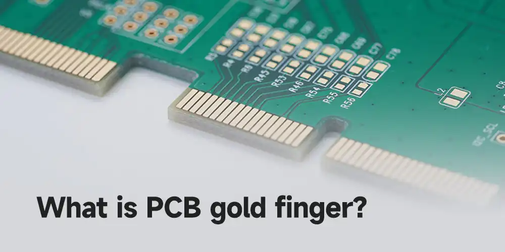
Gold-plated columns, often known as “gold fingers,” are occasionally used to improve connectivity between adjacent layers on printed circuit boards (PCBs). Connecting a supplementary PCB to a computer’s motherboard requires using gold fingers. Smartphones and smartwatches are only two examples of digital-signal transmission gadgets that use gold-plated printed circuit boards (PCBs).
There are three distinct varieties of PCB gold fingers.
1. Common PCB
Widely used PCB gold finger layout with a regular and uniform distribution. All of the pads on the PCB are the same size and distance apart.
2. Thin PCB
The PCB pads are of the same width, although their lengths and occasionally their spacing vary widely.
3. Segmented PCB
Pads on the printed circuit board vary, and the gold fingers are cut into many sections.
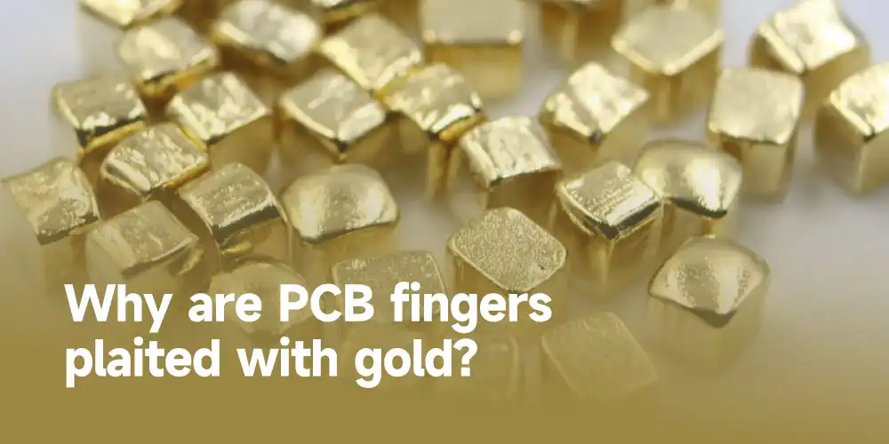
Since gold is so electrically conductive, it is often used for PCB connections. PCB fingers with gold plating offer a reliable electrical connection and shield components from moisture and humidity. It also aids in lowering the contact resistance that might cause signal deterioration or interference.
As a bonus, gold’s durability means it will only need to be replaced for a very long time. Gold plating also prevents oxidation, which may lead to electrical problems like short circuits, so it’s a double bonus. Gold plating, the last step, is visually pleasing and gives your PCBs a polished, expert appearance.
Pros
Cons
Connecting contacts, often gold fingers, are used to join two neighboring printed circuit boards. Aside from its electrical conductivity, gold also acts as a protective covering for the exposed surfaces of the joints.
The endurance of solid gold at its specified thickness enables a printed circuit board (PCB) with gold fingers to be inserted, withdrawn, and re – injected into its appropriate slot a hundred times without causing any damage to the board. This is made possible by the fact that solid gold is used.
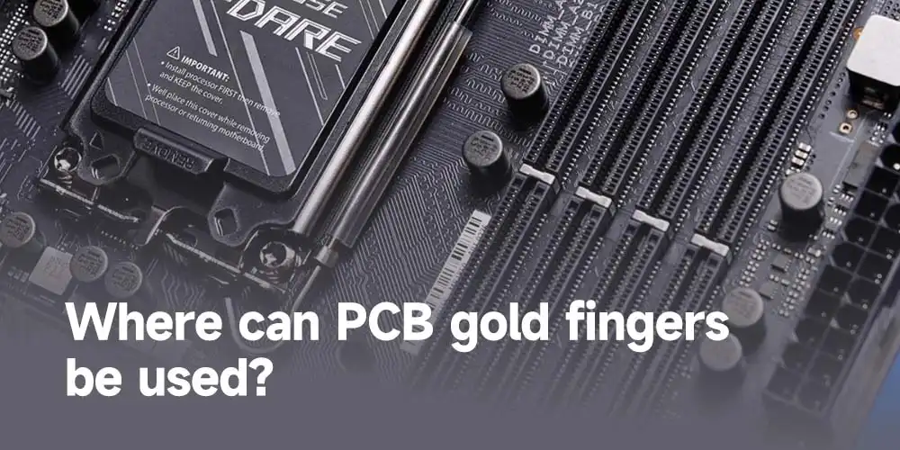
Gold fingers have several purposes. First, PCB gold finger allow a variety of peripherals to communicate with the central system in any particular computer architecture. Typical applications of gold fingers also include the following:
1. Interconnect Points
Female expansion slots, such as PCI, ISA, and AGP, connect expansion boards to the primary motherboard. The gold fingers in these slots transmit data between the computer and an external device or an expansion card.
2. Extraordinary Adapters
You may upgrade your computer in various ways when you have gold fingertips. For example, graphics and audio quality enhancements may be added to a laptop using supplemental PCBs that plug perpendicularly into the motherboard. The gold fingers on these cards tend to outlive the cards themselves since they are seldom detached and reattached.
3. Additional Connections
PCB gold finger connects the expansion cards and other devices to the motherboard. In addition, slots on the back of the PC case accept cables from peripherals such as speakers, subwoofers, scanners, printers, and displays. These slots are connected to the motherboard through PCBs.
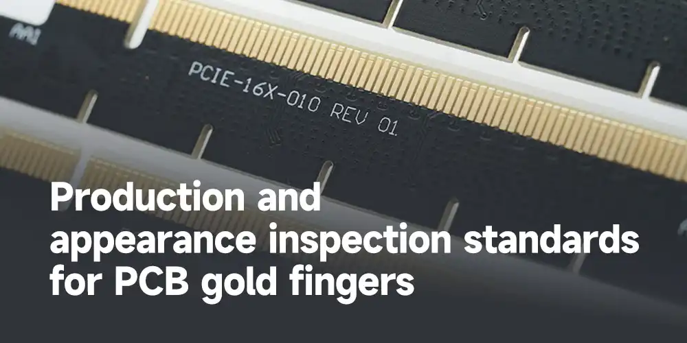
PCB gold finger electroplating is used on circuit boards after the insulation material but before the surface quality. The stages involved in plating are as follows:
1. Process of Plating Nickel on a Surface
The fingers’ connection edges are nickel-plated to a thickness of 3-6 microns.
2. Adding a Layer of Gold
Gold is plated onto the nickel at a thickness of 1-2 microns. In most cases, the gold will have some cobalt added to it to increase its surface resistance.
3. Beveling
The ends of the connectors are cut at exact angles to allow for easier insertion into their corresponding holes. Typically, a beveling angle of 30 to 45 degrees is used.
In a typical circuit board, some gold fingers will be noticeably longer than others. For instance, the fingers on a fuse box may be longer at one end than the other. That’s why the PCB has lengthy fingers at one end; they allow it to snap into position rapidly. The last of the PCB ends are put in, completing the installation.
The plating method has its limitations. For example, some circuit board components, such as the gold fingers, need specific clearances from one another. Among the most important limitations are the following:
The copper in the inner layers must be kept out of the PCB edge during the beveling process.
Printed circuit boards need precise spacing around their gold fingers, and any variation from this standard might weaken or even render the card useless.
1. Blue Glue Coverage
Most printed circuit board (PCB) is coated in blue glue, but the gold finger pads (which need rigorous gold plating) stand out. Furthermore, they ensure that the conductive location is aligned with the board’s intended use.
2. Cleaning the Copper of PCB
First, they use sulfuric acid to remove the oxidation layer from the PCB pad, and then we use water to rinse the copper. The PCB pad’s surface is then ground to remove any remaining residue. The copper surface is next washed down with water and deionized water.
3. Nickel Plating on Copper PCB Pads
They next activate the electroplating process, adding a nickel coating to the surface of the polished gold finger pads. The surface of the nickel-plated pad is then cleaned with water and deionized water.
4. PCB Pad Electroplating with Gold Over Nickel
After nickel plating the PCB pad, they start electroplating to add the gold layer. Gold that can’t be reused is recycled. Next, they wash the gold off our fingers with water; last, we use deionized water.
5. Take Away the Blue Glue
All the gold fingers on the PCB have now been plated hard gold. Once the blue glue has been removed, the PCB assembly may print the solder mask.
So that’s about everything you need to know about integrated circuits and how they work. We at Qtech are always ready to give you solid advice about PCBs, PCBA, and ICs. Talk to us today and find out more on what we offer. With over a decade of experience in this field, you’re guaranteed quality always.