blogs
Qtech Technology Co., Ltd
SMT / DIP / PCB assembly /
Testing / BGA reworking
QUOTE
close
SMT / DIP / PCB assembly /
Testing / BGA reworking

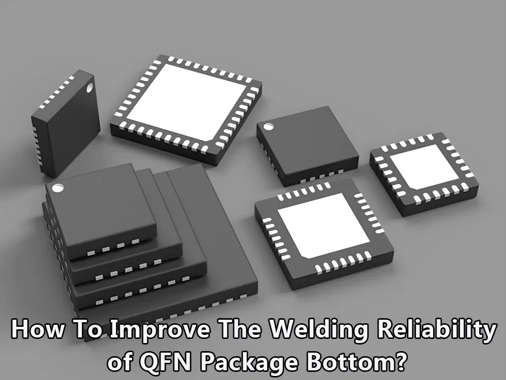
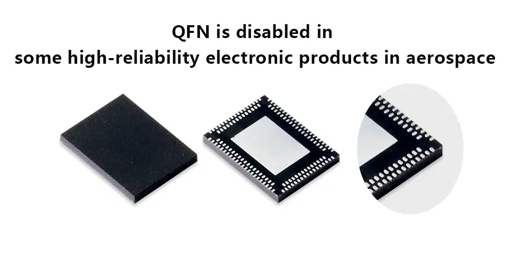
The feature of QFN without pins makes QFN can only be connected to the PCB pads through the device’s own grid. On the one hand, it cannot absorb the stress caused by thermal mismatch through the deformation of the pins. On the other hand, the grid is blocked by the device, which brings challenges to the detection and reliability of solder joints.
Experiments have shown that when the solder filling thickness of QFN is less than 0.1mm, the hidden danger of solder joint reliability is greater. And it is necessary to further adjust the welding process and PCB pad size to improve solder joint reliability.
The fundamental reason why QFN is disabled in some high-reliability electronic products in aerospace is that QFN does not have pins that can provide buffering effects for solder joints in a mechanical environment (such as printed circuit board deformation). Incoming shear force caused by printed circuit board deformation is directly and repeatedly applied to the solder joint, causing the solder joint to crack.
QFN leads to cracking of solder joints under a certain mechanical environment. It is only an expedient measure to prohibit the use of QFN package. The anti-vibration capabilities of devices are very limited and small. And it is particularly necessary to further strengthen the overall anti-vibration capability design of products using QFN devices. Therefore, there is no reason to blame the device for the defects caused by inaction in the anti-vibration design of the product structure.
1. Removal of gold and tinning treatment
The surface of the heat sink at the bottom of the QFN device and the surrounding pads are all gold-plated. Before soldering with tin-lead solder, the gold-coating and tinning must be completely removed to make the solderable plating area greater than 95%.
2. Ensure the soldering reliability of the heat dissipation pad
There is a large heat dissipation pad at the bottom of the QFN. When the heat dissipation pad is not soldered to the PCB, the board-level reliability is reduced by 20%.
3. Increase the package clearance height to improve board-level reliability
The package clearance height is defined as the distance between the pad on the bottom of the QFN substrate and the pad on the surface of the PCB. The package clearance height should be verified and a process specification should be established to ensure the clearance height.
The package gap height varies depending on the amount of solder paste on the pad. When the QFN is soldered to a printed board, the flux and solvents in the solder paste will separate from the alloy. After reflow soldering, the gap height is about 50% of the original solder paste thickness; PCB design should be conducive to forming a suitable package gap height, and after reflow soldering, a solder fillet thickness of 50 μm can help improve reliability.
4. The thickness of solder filling requirements
In order to ensure a robust connection interface between QFN and PCB, the shape of solder paste must be strictly controlled.
Excessive solder paste volume or uneven solder paste deposition can cause components to float, resulting in pad misalignment, irregular bridging and voids. Insufficient solder paste will affect the reliability of the product. Even the smallest bending deformation of a component or PCB can result in an open solder joint.
The solder filling thickness refers to the solder filling thickness between the pad at the bottom of the QFN and the pad on the PCB surface after QFN reflow soldering. The solder filling thickness of QFN is less than 0.1mm, and the reliability of the solder joint is relatively large, so it needs to be adjusted. Soldering process and PCB pad size improve the reliability of solder joints.
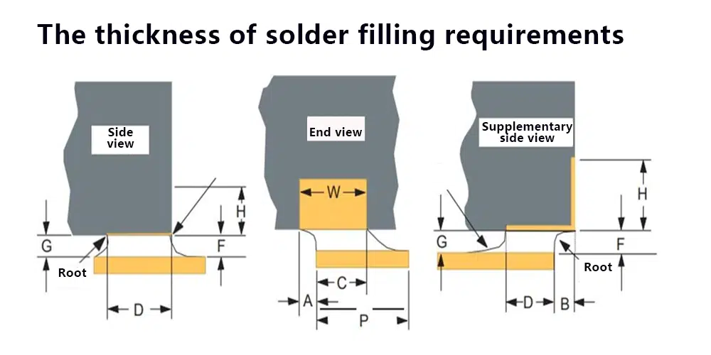
(1) QJ3086A bottom terminal chip component solder filling height G=0.1~0.4mm.
(2) QJ3011A bottom pad The height of the solder filling at the bottom of the solder end of the chip component is G=0.1~0.4mm.
(3) QJ165B solder fillet thickness G is good wetting.
(4) The IPC-610G solder filling thickness G is obviously wet and filling, which cannot meet the requirements of high-reliability electronic products for QFN welding.
(5) IPC-7093 requires that the solder filling thickness of QFN should generally be between 50 μm and 75 μm after reflow soldering.
(1) The formation of the solder filling layer depends on the surface assembly process.
Variables that affect solder fillet formation are: the activity level of the solder paste and flux used, PCB pad size, the amount of solder paste printed, and the height of the component from the board.
(2)In order to achieve the preferred 50μm thickness solder joints, the recommended solder coverage should be ≥ 50% for plug hole types and ≥ 75% for trespass hole types.
(3)The formation of fillet is related to PCB pad size, printed solder paste volume and gap height. The gap height of QFN package components and PCB pad size will affect the required solder volume.
(4)Packages with a larger silicon die/package ratio, resulting in a solder fillet, can improve board-level product reliability by as much as 2x. Reliability is improved because the solder fillet extends the solder joint length.
However, the formation of the solder filling layer and the height from the board are not independent of each other. If the height from the board is less than 0.05mm, even if the solder filling layer is formed, the reliability of the solder joint cannot be increased that much.
(5)Since the exposed terminal cutouts of most vendors’ unshrunk QFN components are unplated copper, the bare copper will eventually oxidize and interfere with solder wetting during reflow. Additional measures are required to plate or coat exposed copper terminal cutouts to ensure solder wetting.
(6)The formation of solder fillet depends on the solder paste (flux) used and the degree of oxidation. The formation of solder fillet is also related to the size of the PCB pad, the amount of printed solder paste and the height of the package gap.

①G increases with the increase of the amount of solder paste on the heat dissipation pad at the bottom center of the QFN.
②G is related to the vias on the exposed pad around the bottom of the QFN.
③G increases with the adoption of via fill in the bottom center thermal pad of the QFN.
④ G is dependent on the amount of solder wetting or flowing into the plated via.
⑤The solder mask is allowed to cover the pad, but the via hole is not filled – the “intrusion hole”, which provides a channel for the solder to easily flow into the via hole to reduce G, while the plug hole is due to the end of the via hole It is plugged closed, preventing the flow of solder into the via hole.
⑥Intrusion hole design, number of vias and size of surface treated vias also affect clearance height.
⑦G is related to the type of solder paste used for soldering and chemical reaction, PCB thickness, PCB surface treatment and reflow soldering curve.
⑧G is related to the weight of the QFN device, the amount of solder paste, the size of the pad, and the structure of the pad (solder mask limited or non-solder mask limited).
⑨G varies with the wettability of the solder paste.
⑩G changes with the inflow of solder paste into the PTH hole: the windowed via hole will allow the solder to easily flow into the PTH and reduce the gap height, while the filled via hole prevents the solder from flowing into the hole because the two ends of the hole are filled. In addition, for windowed via designs, the number of vias and the size of the holes after surface treatment will also affect the thickness G.
In order to meet the requirements of G>0.1mm, various measures can be taken to form the suitable thickness G based on PCB design considerations.
① Using a thick template can increase the thickness “G”, but due to the increase in the solder paste release area ratio, the height is limited.
② QFN device pad solder “bump” when multiple components are mounted on the same board, the thickness of the template cannot be suitable for only one or two components. The bump QFN package is selected, and the pins are plated to protrude. The board-level reliability of the QFN package is increased by 2 times.
③ Central thermal pad design, amount of solder paste coverage, number and size of vias have a great influence on the clearance height.
④ Increased solder fillet thickness can be achieved with a thicker stencil, but this option is limited because of the requirements for the stencil width-thickness ratio and area ratio for solder paste release and center pad floating.
⑤In order to meet the requirement of solder filling thickness greater than 0.1mm, you can design a stepped template or choose solder paste printing technology.
Solder fillet thickness depends on the amount of solder paste on the pad. When the QFN is soldered to a printed board, the flux and solvents in the solder paste will separate from the alloy. After reflow soldering, the solder fillet thickness is approximately 50% of the original solder paste thickness.