blogs
Qtech Technology Co., Ltd
SMT / DIP / PCB assembly /
Testing / BGA reworking
QUOTE
close
SMT / DIP / PCB assembly /
Testing / BGA reworking

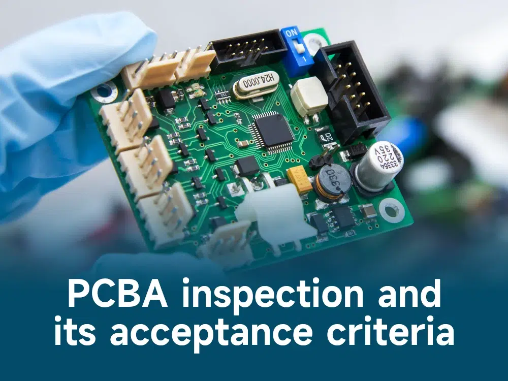
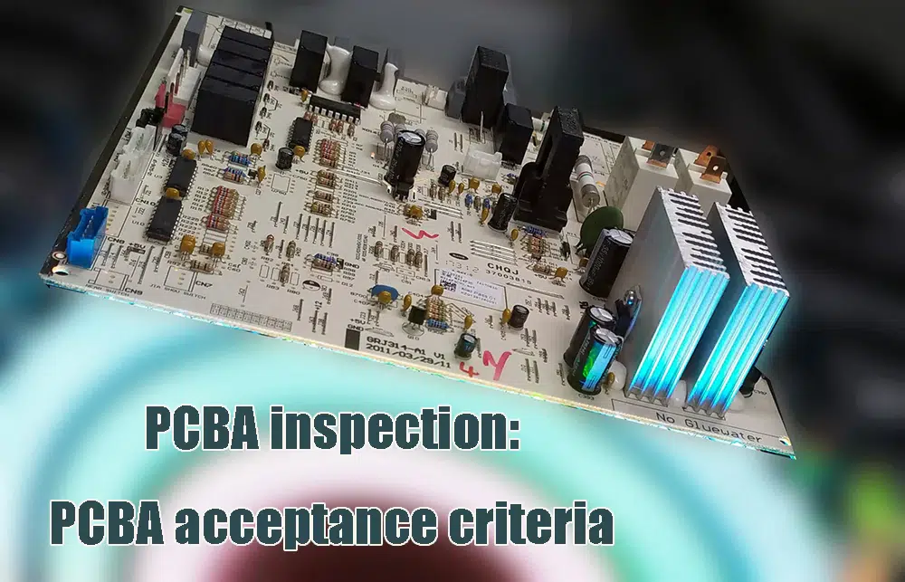
Printed circuit board assembly PCBA inspection is a critical process in electronic device manufacturing. It involves checking the quality of PCBs and their components to ensure that they meet the necessary specifications and standards. PCBA inspection is an important aspect of quality control as it helps prevent defects and failures in the final product. In this article, we will discuss the inspection and acceptance criteria for PCBA board in detail.
The PCBA inspection process usually involves a combination of automated and manual inspections.
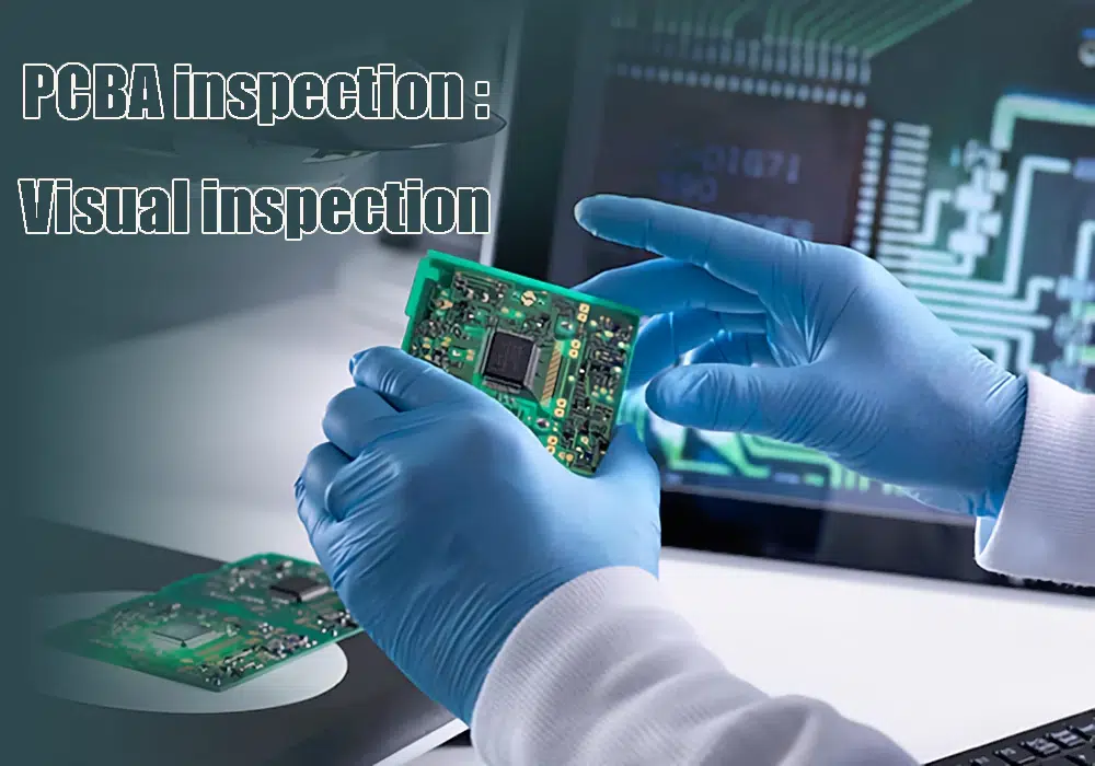
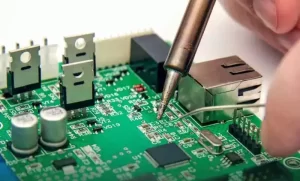
The first step in the process is a visual inspection, typically after the SMT placement process is complete, that includes checking the board for any physical defects, such as cracks, scratches, or damage to the solder mask. This is usually done manually by a trained inspector using a magnifying glass or microscope.
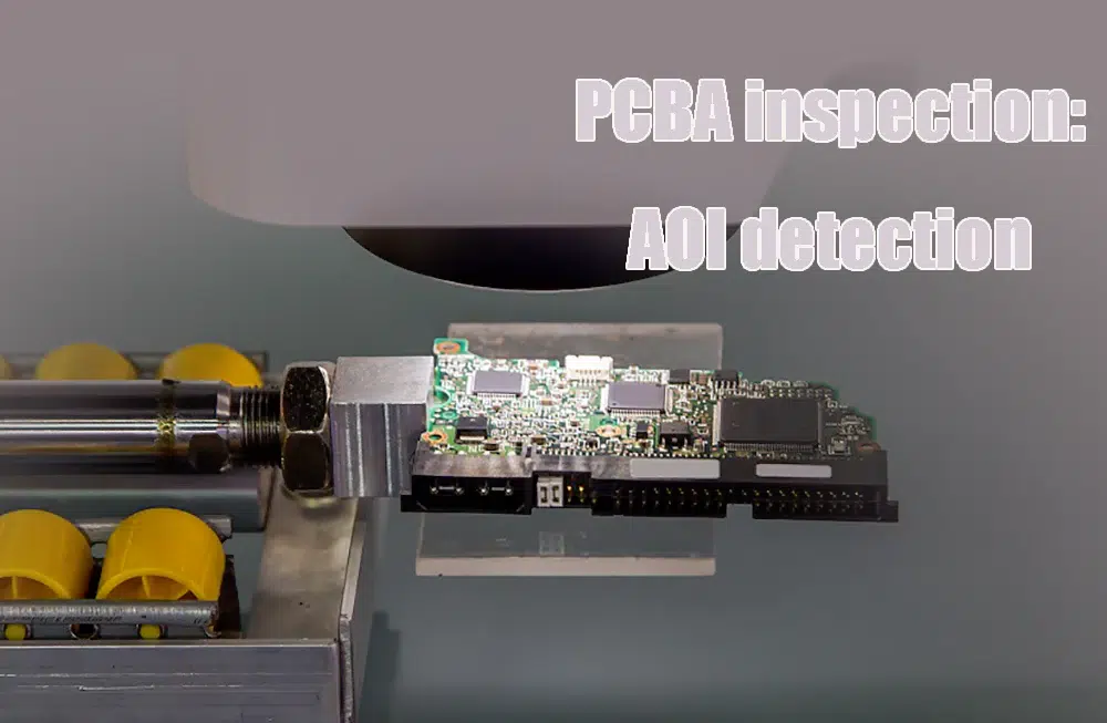
The next step is Automated Optical Inspection (AOI), a non-contact testing method. Automated optical inspection plays an important role in PCBA inspection. Automated optical inspection is an automated visual inspection of printed circuit board manufacturing processes. It uses cameras and software to detect defects such as missing components, misaligned components, and welding defects. AOI is a fast and accurate inspection method that can detect defects that are difficult to identify manually.
● The purpose of AOI is to use optical principles to compare data, conduct inspection, and attach corresponding maintenance and scrapping treatment. There are three main processes.
[1] AOI (Automatic Optical Inspection) . Uses AOI equipment (scanner) to compare data, find out the location that is different from OK products, and record it.
[2] VRS (maintenance). Through the VRS equipment (maintenance machine), check the location of the difference with the OK product one by one, and after judgment, repair or make a mark.
[3] Repair line / scrap. According to the identification made after judgment, the product is scrapped or repaired.
● Time of using AOI
1. Use after the SMT patch processing is completed: it can effectively prevent the lack of components, polarity, shift, tombstone, reverse side and other problems.
2. Use after reflow soldering: at the end of the production line, the detection system can effectively check the missing components, offset, skew and other problems of PCBA processing, the correctness of the solder joint and whether the amount of tin is insufficient, and defects such as soldering short circuit and peeling.
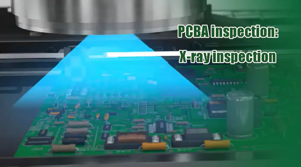
In recent years, area array components such as BGA, QFN, CSP, and flip chips have been more and more widely used in electronic manufacturing. For example, BGA has a smaller pin count, inter-pin inductance and capacitance, and better heat dissipation performance than other components. However, BGA also has disadvantages, such as after SMT, it is difficult to judge the solder quality by naked eye or AOI testing under the package.
In order to guarantee the quality of welding, more and more manufacturers choose X-ray inspection of components with hidden solder joints after AOI.
The board may undergo x-ray inspection to detect defects in hidden areas, such as solder joints underneath surface-mount components. X-ray inspection is particularly useful for detecting defects such as voids in solder joints that would be difficult to detect using other methods.
PCBA acceptance criteria are standards and specifications that a circuit board must meet in order to be considered ready for use in electronic devices. These standards may be developed by manufacturers or regulatory bodies, such as the International Electrotechnical Commission (IEC) or the European Union’s Restriction of Hazardous Substances (RoHS) directive.
Acceptance criteria for PCBA inspection typically include the following:
Solder joint quality – This refers to the quality of the solder joint between the component and the PCB. Criteria for solder joint quality usually include the amount of solder, the shape of the joint, and the presence of any defects, such as voids or cracks.
Component placement – This refers to the accuracy with which components are placed on the PCB. Criteria for component placement typically include the alignment of components, the distance between them, and the orientation of components.
Electrical Performance – This refers to the functionality of the circuit board and its ability to meet the necessary electrical specifications. Criteria for electrical performance typically include the resistance, capacitance, and inductance of the component, as well as the overall performance of the board in terms of signal quality and noise.
Physical Defects – This refers to any physical defect in the circuit board, such as cracks, scratches, or solder mask damage. Criteria for physical defects usually include the size, shape, and location of the defect.
Compliance with regulatory standards – This means that the circuit board complies with regulatory standards such as the RoHS Directive, which restricts the use of certain hazardous substances in electronic devices.
Processability – including appearance, finish, flatness, character cleanliness, via resistivity, electrical properties, heat resistance, solderability and other comprehensive properties.
The PCB board surface can not remain flux, gum and other oil stained lines, no short circuit, open circuit phenomenon.
● Non-line conductors (residual copper) must be more than 2.5mm away from the line and the area must be ≤ 0.25 mm
● Drilling is not allowed in situations such as multiple drills, missing drills, deformations and through-hole penetration.
● PCB layout and PCB pads are not allowed to warp; It is not allowed to have copper and tin on the line.
● PCB is not allowed to break and the panel requires VCUT, its depth must be 1/3 of the thickness of the board.
● The actual line width shall not deviate from ±20% of the original design width. Dimensional tolerance of ±0.15mm. The edge of the substrate is convex or concave≤ 0.2mm.
● The offset of the solder mask and screen printing does not exceed ±0.15mm. No fingerprints, water streaks or wrinkles are allowed on the surface of the solder mask.
● The text on the component surface must not be damaged or illegible. The paint area on the PCB pads must be ≤ 10% of the original area.
● PCB deformation, bending, warpage ≤1% diagonal length of the substrate.
There are several standards used to guide PCBA inspection, including IPC-A-610, IPC-J-STD-001, and IPC-7711/21. These standards provide guidelines for the inspection and acceptance of PCBA and are widely used in the electronics industry.
The IPC-A-610 standard is the recognized standard for acceptability of electronic components. It provides the following criteria for acceptability:
1. Component placement and orientation
2. Solder joint standards for through-hole and surface mount components
3. Solder joint standard for fine pitch components
4. Mechanical assembly standards, including the installation of connectors, switches and other components
5. PCB cleanliness and coating standards
6. The IPC-J-STD-001 standard specifies the requirements for welding electrical and electronic products
So that’s about everything you need to know about integrated circuits and how they work. We at Qtech are always ready to give you solid advice about PCBs, PCBA, and ICs. Talk to us today and find out more on what we offer. With over a decade of experience in this field, you’re guaranteed quality always.