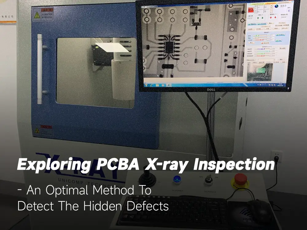
Exploring PCBA X-ray inspection – An optimal method to detect the hidden defects
2023-10-06
Home » service » BGA PCB Assembly » Exploring PCBA X-ray inspection – An optimal method to detect the hidden defects
During PCB manufacturing and assembly, there’s a high chance of manufacturing defects. Some defects are visible by naked eyes, while some require special inspection techniques, where PCBA x-ray inspection is one such technique. In this article, you’ll revolve around PCBA x-ray inspection and all the important details related to x-ray inspection.
What’s PCBA X-ray inspection?
When inspecting a PCB for any defects during the manufacturing process, x-ray inspection can be used. It’s a technique that allows you to get a deeper and better look at your PCB to find defects the size of microorganisms. PCBA X-ray inspection intends to keep the PCB assembly board safe while giving all the insights of any possible manufacturing defects.
Thus, it allows manufacturers to take corrective actions as needed. Many people also call PCBA X-ray inspection as PCBA X-ray testing. This type of testing can be performed in different stages, so as to maintain quality assurance of the PCBA board.
Enables Non-destructive Testing X-ray won’t harm your PCB, so you can stay worry-free about your PCB/PCBA getting damaged during inspection. Moreover, none of the components would get harmed during PCBA x-ray inspection.
Helps Verify Proper Component Placement It’s quite possible that the components on a PCBA might look properly placed but there might be a slight misalignment. To find any improper placement and overcome this issue, PCBA x-ray inspection comes into action.
Gives An Insight Into The PCB Viewing your PCB with your naked eyes won’t reveal many defects. But PCBA x-ray inspection can give you a deep insight without the need for a microscope or any magnifying device.
Helps Achieve Quality Assurance If you can find out and correct any issues and defects in your PCBs before selling it to the clients, you’re assuring quality in your products. Your efforts in quality assurance will play a key role in boosting your business in the long-term.
What are the types of PCBA X-ray inspection?
2D X-ray Inspection In 2D inspection, the inspector takes a 2D image and represents all the components, solder joints, layers, etc., in a top-down view. This’ll help manufacturers verify solder joints, component placement, and identify solder bridges (if any).
3D X-ray Inspection The inspector will take a 3D image of the PCBA and will show you all the layers and internal structure. Several images from several angles might be needed to recreate a 3D image of your PCB.
Microfocus X-ray Inspection The microfocus x-ray inspection clicks images in a small section that helps capture a high-resolution image of a small spot. Rather than taking pictures of the entire PCB/PCBA, a small area or a region is inspected at a time.
Automated X-ray Inspection In the automated inspection, a robotic inspector is deployed for the PCBA inspection. Some inspection machines might be involved along with the robot for better automation testing.
Manual X-ray Inspection When going with the manual x-ray inspection, a human inspector is assigned to the project. He/she will manually place the PCB/PCBA under the x-ray machine and will perform all the test functions.
What are the applications of X-ray Inspection in PCBA?
1.Inspecting BGA and QFN: Quad Flat No-lead and Ball Grid Array are the two components on a PCB. They have solder joints under them, which can only be inspected through x-ray testing.
2.Wire Bond Inspection: Semiconductor devices have wire bonding connections and x-ray testing is used to check the integrity of them.
3.Inspection of Solder Joints: It’s not always guaranteed to have 100% perfect solder joints during PCB making. Therefore, PCBA x-ray inspection serves as an economical way to ensure that no solder joints are loose or damaged.
4.Analyzing Internal Structure: PCBA x-ray inspection is a very great option to check the internal structure and condition of a PCB without damaging it, which isn’t possible with naked eyes or a microscope.
5.Quality Assurance & Customer Satisfaction: PCB makers, who thrive on high-quality PCB delivery always take help of PCBA x-ray inspection to make sure that they put a smile on their clients’ faces every time they deliver PCBs to them.
How PCB X-ray inspection work?
Setting Things Up
Engineers choose an x-ray inspection method and set up tools needed for the process.
The PCB is placed under the x-ray machine.
Generating X-rays
The x-ray machine emits high-speed electrons to the metal target and when these electrons are reflected by the target, x-rays are produced.
If you want to get a deeper insight into the PCB, then the x-ray machine needs to be adjusted a little bit. Then it’ll allow x-rays to penetrate in the surface and reveal the insights of the PCB.
Different materials on the PCB will absorb x-rays in different amounts. The amount of x-ray absorption is later helpful for the engineers during analysis.
What are the common defects that PCBA x-ray inspection can detect?
1.Improper or Insufficient Solder: Sometimes there can be a lack of solder on a joint that can cause a short circuit and/or overheating in the PCB/PCBA.
2.Cold Solder: Even if you’ve applied enough solder on a joint, it’s possible that the joint has not bonded nice and tight, which is termed as “cold solder”.
3.Solder Bridging: Solder bridging is an annoying defect that results in an unwanted connection between two pins and/or components on a PCBA.
4.Tombstoning: Tombstoning is a situation when a component on your PCBA gets lifted from one side, resulting in a misalignment. (Under the right circumstances, the component’s base is parallel to the PCB, while in tombstoning, the gap between the component and PCB is different at different points). X-ray inspection can help detect that.
5.Void in Solder Joints: Any air bubbles or gaps in the solder joint will create a weak bond and will impact the overall mechanical strength of the PCB. This can lead to overheating and/or short circuit.
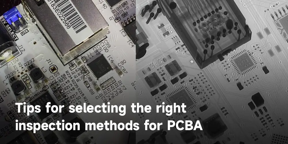
How to select the right inspection methods for PCBA?
There are several types of PCBA x-ray inspection, but which one suits you? Let’s see!
Learn About Inspection Types First First you must learn and get an idea of all the types of inspection techniques trending in the market. That’ll help you figure out which one suits you the most.
Consider Your PCB’s Complexity If your PCB is simple, then 2D testing would be enough. But if your PCB has fine components and the number of components, joints, and traces is high, then go for automated or microfocus testing.
Consider Your Production Volume If you have bulk PCB order, then manual testing would increase the delivery time. Therefore, go for automated testing. If the production is low, then manual testing would be of great help.