blogs
Qtech Technology Co., Ltd
SMT / DIP / PCB assembly /
Testing / BGA reworking
QUOTE
close
SMT / DIP / PCB assembly /
Testing / BGA reworking

Understanding PCB is a prerequisite to learning about single-layer printed circuit boards (PCB). PCB is an abbreviation for “printed circuit board,” which describes a board used to link various electrical components through pads, tracks, and lines.
In this article, you can learn something about single-layer PCBs. Some single-layer PCB manufacturer’s selection suggestions will also provide.
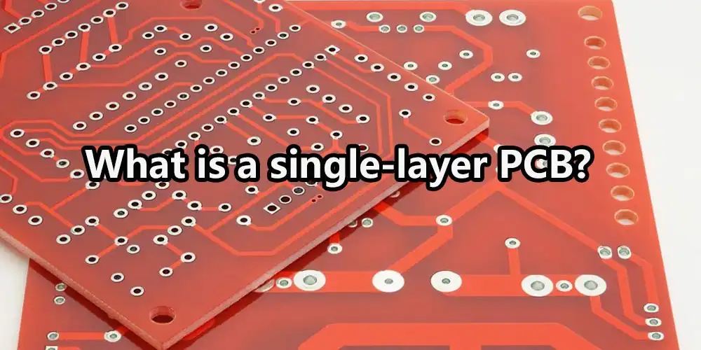
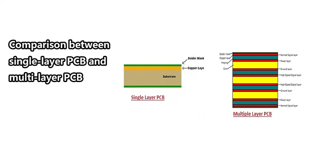
Single-layer PCB is the most fundamental type of PCB and is usually used in the early day. It consists of only one conducting layer (copper) on one side and the other side to incorporate other electronic components.
Above the substrate, there is a single layer of copper conductors. The electrical components will be connected or placed on one side of the board while the other will show the fully etched circuit. The layout and production of single-layer PCBs are straightforward. As a bonus, these PCBs have the lowest production costs.
Because the conductive paths are all in one direction and can’t cross or overlap due to only one conducting layer. This makes these PCBs an option for applications where space is at a premium.
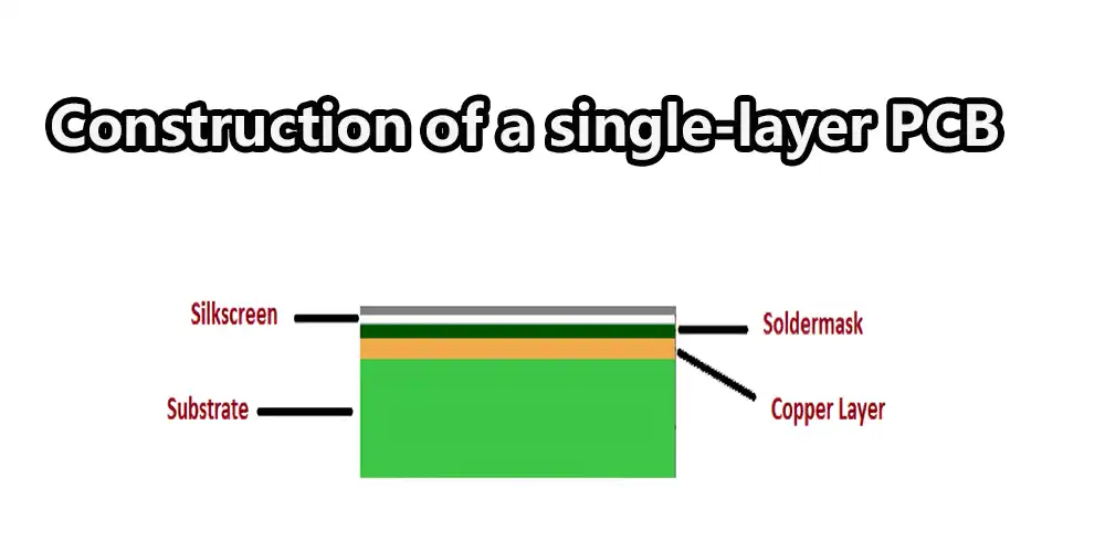
Insulating fiberglass, which is compact in appearance and PCB-strong, serves as the substrate. In addition, the kind and composition of the base material vary depending on how much the board is pliable or stiff.
Above the substrate, a copper sheet is a conducting channel for the different components on the board. Naturally, the amount of copper on a board varies from one manufacturer to the next and is measured in ounces per square foot.
On the one hand, copper foil is covered with a solder mask layer. The layer’s primary function is to insulate the copper foil, preventing conduction in accidental contact with a conducting substance.
However, a silkscreen layer sits atop all other layers, and its primary function is to add characters and symbols to the board, making it more legible and straightforward to decipher.
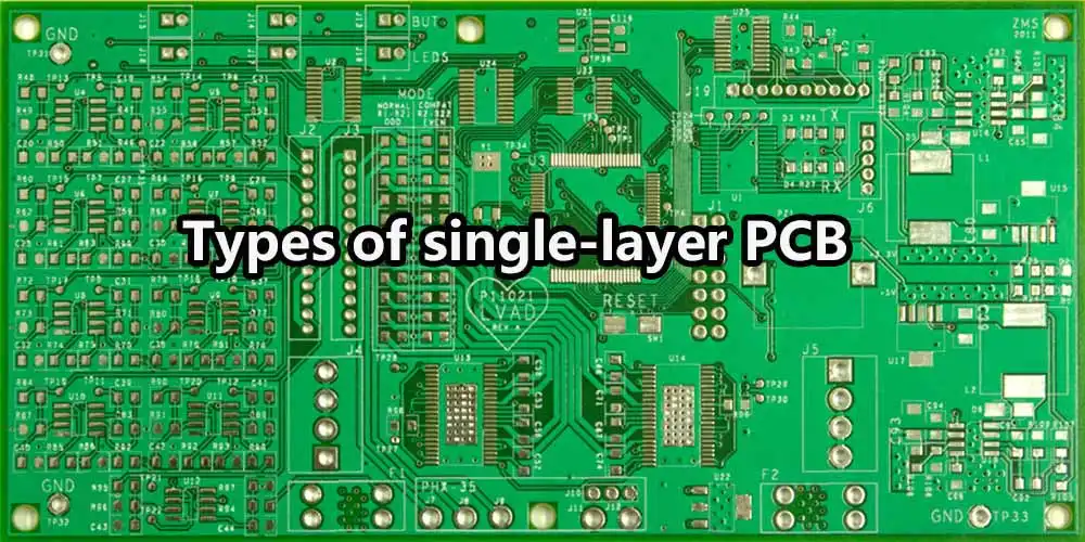
There are five different types of single-layer PCBs in the market.
It’s the kind of single-layer PCB you can only build out of stiff stuff like fiberglass. The rigidity of the circuit boards protects them from damage caused by bending or breaking. They are now common in much electronic equipment, including power supplies, calculators, and more.
It’s a variation of single-layer PCBs that uses a flexible material rather than a rigid one. In addition, they use plastic components. Even though they’re more expensive, single-layer flexible printed circuit boards provide some benefits over their rigid counterparts.
PCBs of this sort are often employed at frequencies up to several gigahertz and represent a particular case of single-layer boards. The circuit boards are constructed from Teflon or polyphenylene oxide (PPO). When shopping for high-frequency single-layer PCBs, it’s essential to consider factors like thermal expansion, dielectric loss, water absorption, etc.
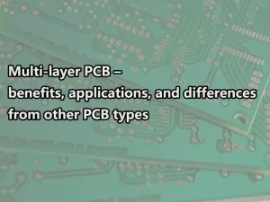
It’s the kind of single-layer PCB that combine glass fibers and plastic. Consequently, plastic and fiberglass are examples of single-layer materials. Compared to single-layer rigid and flexible PCB, multilayer boards offer several benefits, including a smaller footprint and less weight.
It’s an aluminum substrate PCB with a single insulating layer. The boards’ layout is similar to that of copper-backed PCBs, but the latter uses a copper substrate while the former employs an aluminum one.
High pressure and heat bond the prepreg layers and base material in multi-layer PCBs.
Several CNC machining operations are typically used to fabricate the single-layer PCB. Cutting, drilling, placing graphics, etching, putting on a solder mask, and printing are all part of the process.
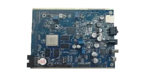
A single-layer PCB is suitable for some easy tools, whereas a multi-layer PCB is better suited to complex electronics like smartphones.
Metal, FR-4, CEM, Teflon, and polyimide produce single-layer PCB and multi-layer PCB. Still, copper tends to be the metal of choice in such situations.
The cost of production is lower for a single-layer PCB than for a multi-layer PCB. Reasons for this include high-quality raw materials, extensive processing time, and skilled labor.
It needs to be more sophisticated for intricate tasks.
Due to their cheap production cost, single-layer PCBs are used in many common appliances and consumer devices. These are often used in devices with limited storage capacity. A few of them are as follows.
Laser direct imaging (LDI) can be used to apply the regions that will become the trace, pads, and metallic ground of the printed circuit board to a multi-layer PCB before any other work is done on the board.
After all the layers of a PCB have been etched away, the interior layers are given a chemical method called oxide to strengthen the binding. Then, a hydraulic press is used to heat the laminated layers, which alternate between prepreg and copper foil.
By drilling or lasering through the layers of a multi-layer PCB, vias may be created to carry signals across the layers. It’s best to drill on a stack of two or three panels at once; however, this varies with the type of through used.
Chemical and mechanical procedures remove excess glue and debris from the surface after holes have been drilled into it.
After the protective covering has been peeled away, a metal substrate for electroplating may be formed by applying a thin layer of copper to all exposed areas of a panel.
After the panel has been prepared by drilling holes and exposing the conductive pattern, it is submerged in a bath of copper sulfate and sulfuric acid to produce copper plating.
Now, shield the PCB with a solder mask utilizing the same ultraviolet (UV) exposure seen in the photoresist step before going on to the PCB assembly stage.
Now that the PCBs have been fabricated, they must be tested and examined thoroughly to verify their functioning before they can be assembled and sent.
Designing a single-layer PCB is simple if you consider these guidelines.
It is the vias, in a nutshell, that allow for the various connections between the multiple layers of the boards. Since the thickness of the panels varies, you may need to use multiple vias depending on the kind of board you’re working with. You may choose between Blind, Through-the-Hole, Buried, or Micro.
The amount of copper used in a circuit board’s traces is expressed in ounces. Most PCB designers utilize just a few ounces of copper; however, some PCB manufacturers may provide boards with as much as six ounces of copper if necessary.
NOTE: Keep in mind that issues with lamination and soldering might arise from using the incorrect trace thickness.
Building a rudimentary stacking guide for your PCB is essential for figuring out even the most fundamental aspects of your board. The complexity of the PCB will decide how much you will spend time and money on its fabrication and the raw materials required.
To guarantee that your fabricated PCB meets your specifications, you must always specify those specifications in advance. Component placement, layer assignment, duration of flight analysis, and engineering time should all be factored in.
Observe the rise and fall timings of the signals, the impedances, the track lengths, and the intensity of the drives. Test before and after the layout to see whether your efforts paid off.
So that’s about everything you need to know about integrated circuits and how they work. We at Qtech are always ready to give you solid advice about PCBs, PCBA, and ICs. Talk to us today and find out more on what we offer. With over a decade of experience in this field, you’re guaranteed quality always.