blogs
Qtech Technology Co., Ltd
SMT / DIP / PCB assembly /
Testing / BGA reworking
QUOTE
close
SMT / DIP / PCB assembly /
Testing / BGA reworking

The term “trace” is often used to describe the interconnected system of copper, wire, insulation, and fuses that make up a printed circuit board(PCB). As a rule, if electrical equipment is malfunctioning somehow, it is quite likely that now the PCB trace is inconsistent.
Electronic engineers often use the phrase “trace resistance” in the PCB business. Components of a printed circuit board that act as barriers to the free flow of electricity are known as traces.

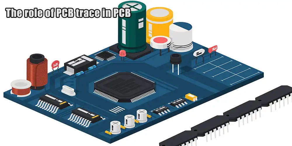
Trace on a PCB is just a list of the many components that make up the board. The trace, like the current, is an unavoidable component of PCB combinations and facilitates the simple resolution of abnormalities. The PCB is one of the ubiquitous parts of every electrical device.
They have become so ubiquitous in modern technology that you can’t imagine a device without them. This makes knowing the trace layout very important. If not, it might compound the problems and need much more work and money to correct. Therefore, acquiring a set of functions and formulae is practical to complete the work quickly and accurately without risking making the same error again.

Traces carry electrical impulses. Hence, the substance used to create them must be highly conductive and sturdy. Copper is the most common material for PCB trace; however, other materials may be utilized. Aluminum or even gold may be used to make a trace.
With effective impedance management, the intensity of a signal flowing along a trace is kept within an acceptable range by adjusting the size and placement of PCB traces to the qualities of the substrate material. Engineers are forced to cope with signal integrity (SI) difficulties as the switching rates of more and more devices continue to grow. As a result, PCB trace can no longer be thought of as a direct link between two points. Traces must be treated as transmission lines to reduce or remove the effect on SI, and impedance matching must be performed. Many possible signal integrity concerns may be avoided or reduced by adhering to sound design techniques and methods.
A PCB trace’s job is to carry electrical current from the device, sending the signal to the one receiving it. Down the trace, power must be sent. However, matching impedances on the PCB are necessary to produce optimum signal power. As a result, impedance matching is necessary. As much of the driver’s power as possible should reach the receiver.
High-frequency signals will certainly deteriorate as they travel from the driver to the receiver if the PCB layout stage is not attentive. The resulting signals will seem quite garbled on an eye diagram, with fluctuating strengths as they travel from source to sink.

Components on printed circuit boards are connected to the different connections through electrical traces. Those are the continuous copper tracks on a PCB. The proper operation of the PCB trace relies on the size of the traces. As the electrons go through the copper, they generate a great deal of thermal energy. The temperature of your board may be managed by adjusting the trace width. For electricity to flow more smoothly, a broader trace is preferable.
It is possible to use the predetermined default trace width when designing a PCB. However, the board may benefit from a different trace width than the one used by default. The current carrying capacity is a key consideration when selecting a trace width.
The link between PCB trace width and current carrying capacity can only be understood with the help of a current table. This partnership allows you to determine how comprehensive your traces need to be on the PCB you’re designing. The maximum current may flow through the trace without surpassing its maximum temperature rating and is therefore referred to as the current carrying capacity.
| PCB trace width | PCB trace current |
| A trace width of 6mil (or 0.152mm) is the bare minimum for most factories. The manufacturing method (etching) and desired output are responsible for this restriction. We utilize 10-12 mil (0.254-0.3 mm) traces to allow some wiggle room. | Less than five miles (0.005″) in width Lower than five-millimeter trace spacing. Holes for vias having a diameter of fewer than 8 micrometers. Sub-ounce or ounce-thickness traces (which equates to 1.4 mils) |
| Minimum PCB clearance (the clearance between any two wires) for general-purpose devices is 0.1 mm according to IPC 2221 standards. | This minimum PCB Trace Current spacing of 0.13 mm (or 5.1 mils) applies to power conversion components. |
| Trace width clearance on a PCB refers to the distance between adjacent traces and the width of the traces themselves. | Whereas clearance refers to the smallest distance between two conductor traces in the air, creepage refers to the shortest distance of conductor traces on a PCB along the surface of the insulating material. |
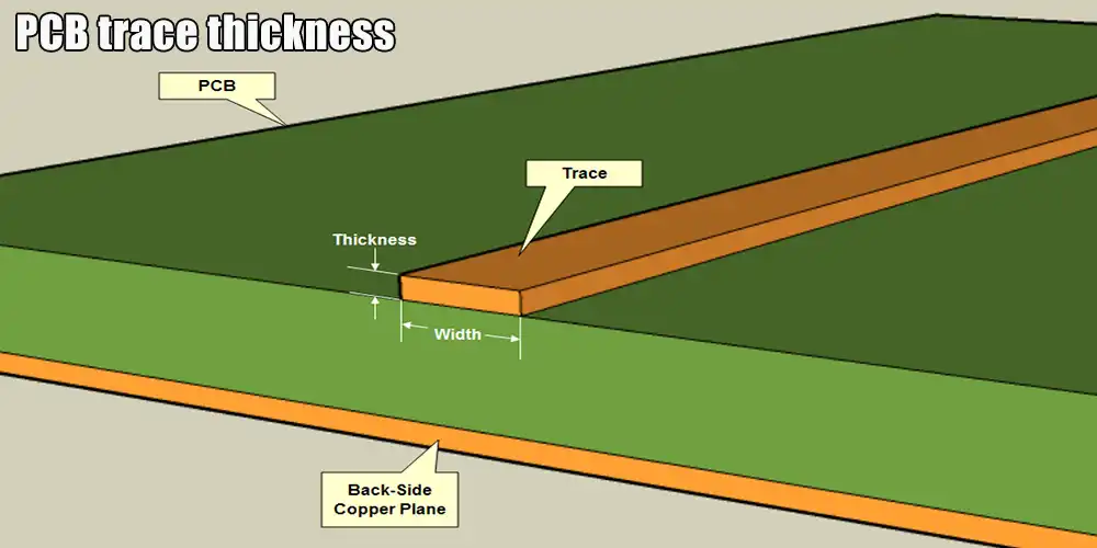
Typically, PCB manufacturer will set the thickness of this kind of copper layer. PCB traces are measured in US units of grams per square foot.
Because of our design, we can control the trace width independently of any other parameters. The industry norm for required trace width is 6mil. Thus, most manufacturers adhere to this (or 0.152mm). This limitation results from the manufacturing process (etching) and the intended effect. To give ourselves a little wiggle room, however, we choose 10 to 12 mil (0.254 to 0.3 mm) traces in width.
In PCB trace design, trace width is a crucial design element. To prevent your board from overheating and melting, you need wide enough traces to carry the current you need. This online calculator will help you determine the smallest trace width required for a certain current and copper weight. Thicker traces are needed for larger currents, but heavier copper allows thinner traces.

It takes a wide variety of knowledge and expertise to maintain or repair a PCB in any of its many possible forms. Repairing PCB trace paths may include replacing the metal, eliminating it, or covering it with a protective coating. The use of heat guns and soldering irons, among other things, are commonplace in these situations.
To make efficient and timely alterations, it is essential to have the proper equipment for repairing circuit board traces. You may fix the PCB trace using the following instruments.

The copper in a circuit board’s traces may be expressed in ounces. In general, one or two ounces of copper is used by PCB trace designers, however certain PCB manufacturers may give up to six ounces of thickness if necessary. Keep in mind that issues with lamination and soldering might arise from using the incorrect trace thickness.
Making an introductory stacking guide is essential for figuring out even the most fundamental aspects of your PCB. The complexity of the PCB trace will govern the materials and labor required for its production, which has, in turn, will set the price.