blogs
Qtech Technology Co., Ltd
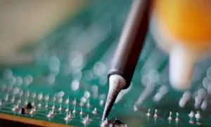
SMT / DIP / PCB assembly /
Testing / BGA reworking
QUOTE
close
SMT / DIP / PCB assembly /
Testing / BGA reworking


PCB anti-static design is a crucial aspect of electronic circuit board development. It involves implementing measures to prevent static electricity from damaging the components and functionality of the PCB. Static electricity, which is an accumulation of electric charge on the surface of an object, can pose a significant threat to sensitive electronic components on a PCB. When not properly controlled, static discharge can cause irreversible damage to integrated circuits, transistors, or other delicate components, resulting in malfunctions or complete failure of the circuit board.
To combat this issue, PCB anti-static design focuses on incorporating various techniques and materials to dissipate or divert static electricity away from sensitive areas. This can include the use of anti-static coatings, grounding techniques, and placement of protective components like ESD (Electrostatic Discharge) diodes.
Static electricity is a kind of electric energy. It exists on the surface of objects and is a phenomenon that occurs when positive and negative charges are locally unbalanced. For example, friction electrification is an electrostatic discharge phenomenon.
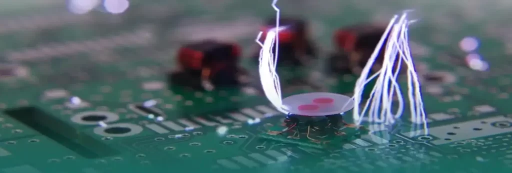
The problem of static electricity has always plagued many electronic products. The electromagnetic field generated by the discharge current has caused serious interference to the circuit through capacitive coupling, inductive coupling, or space radiation coupling. Therefore, we must consider PCB anti-static design in the early stage of PCB design.
When doing PCB layout, put the ESD protection device as close as possible to the input terminal or connector, and the line distance between the ESD protection device and the protected line should be designed as short as possible.
For PCB design, it is very important to set a certain isolation distance on the edge where electrostatic discharge is easy to occur. For rack products, the breakdown distance of electrostatic voltage per kilovolt is about 1mm. 3~5mm isolation area can resist 3~5Kv electrostatic voltage.

1) The wiring should be horizontal and vertical, and the signal lines should be routed side by side as far as possible;
2) If space permits, the thicker the wiring, the better;
3) Carry out wiring according to the high-speed circuit design concept;
4) Avoid processing important signal lines on the edge of the PCB, such as clocks, reset signals, etc.;
5) The conductive loops of all PCB boards, including power and ground loops, should be as small as possible;
6) For single-sided or double-layer PCB, in the absence of a power plane, a ground wire must be followed next to the power wiring;
7) Try to use multilayer PCB wiring.

1) The wiring needs to have a good ground plane;
2) Keep sufficient spacing, such as filters, optocouplers, AC power lines and weak signal lines;
3) Long-distance wiring plus low-pass filter (C, electrostatic device, RC, LC);
4) Isolation (increase the shielding cover), avoid the protected wires and unprotected wires running side by side;
5) Avoid using the same loop with other devices to connect to the common ground point.
1) Keep the integrity of the ground, increase the discharge area of the ground, spread copper evenly on the ground, keep the resistance value of the ground unchanged, and the ground planes in the horizontal state between each other are stable;
2) The periphery of the board is designed around the ground, and the data lines are surrounded by ground;
3) The more ground holes the better, and make each layer of ground tightly connected together;
4) Installing an optocoupler or transformer on the PCB, combined with dielectric isolation and shielding, can well suppress the impact of electrostatic discharge;
5) The GND of the PCB and the ground of the shell can be grounded at a single point to prevent the voltage generated by the electrostatic discharge current on the chassis from coupling into the circuit, but attention should be paid to the selection of the grounding point, and the grounding should be at the cable entrance;
6)If the PCB area allows, and the lap connection and electrostatic discharge channels of the whole system are good, a grounding protection ring can be set around the PCB, which can be treated with bare copper and connected with many vias.
PCB anti-static design is crucial for protecting the investment in electronic components and ensuring the longevity and reliability of PCBs. By taking preventative measures of PCB anti-static design, we can minimize the risks associated with electrostatic discharge, ensuring product quality.