blogs
Qtech Technology Co., Ltd
SMT / DIP / PCB assembly /
Testing / BGA reworking
QUOTE
close
SMT / DIP / PCB assembly /
Testing / BGA reworking

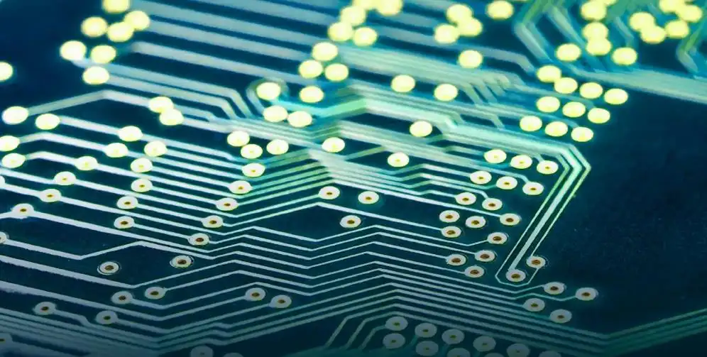
Printed circuit boards (PCBs) are essential parts of contemporary electronic systems and gadgets. They can be harmed by a number of things, though, including physical strain, the environment, and electromagnetic interference (EMI). To maintain their dependable performance and lifetime, PCBs must be protected from such damage.
This article examines the many approaches and concepts of PCB shielding, which protects the PCB from EMI or RFI by employing shielding materials or shielded enclosures. Electronic equipment may retain peak performance and steer clear of EMI interruptions by comprehending the significance of PCB shielding and taking the proper precautions.
A printed circuit board (PCB) can be protected in a variety of ways. The PCB must be treated carefully during the construction, installation, and maintenance phases. By avoiding excessive bending, twisting, and falling of the board, physical damage to the sensitive components and traces on the PCB can be prevented. Adequate grounding procedures should also be implemented to decrease the risk of electrostatic discharge (ESD) damage. Grounded workstations, ESD wrist straps, and ESD-safe handling equipment are required.
Furthermore, it is vital to protect the PCB from severe environmental conditions such as moisture, dust, and temperature changes. These factors can be mitigated by using conformal coatings or a protective case on the PCB. Last but not least, harm brought on by high current flow can be avoided by installing suitable overcurrent protection, such as fuses or circuit breakers.
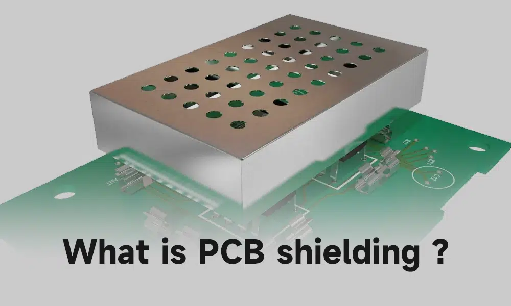
By surrounding a printed circuit board in a protected enclosure or by utilising shielding materials, PCB shielding refers to the technique of defending it against electromagnetic interference (EMI) or radio frequency interference (RFI). The electromagnetic waves won’t interfere with the PCB’s operation or cause unwelcome noise or disruptions since the shielding enclosure or materials are made to block or absorb them.
By reducing the effects of electromagnetic interference, PCB shielding aims to assure the dependable operation of electronic systems and equipment. Different electromagnetic sources, such as adjacent electronic gadgets, power lines, wireless signals, and others, can produce EMI. When EMI enters a PCB, it can interfere with the circuit’s regular operation, resulting in mistakes, signal deterioration, or full device failure. These electromagnetic waves are helped to contain and manage by PCB shielding, which lowers the possibility of interference and boosts the general efficiency and dependability of the electronic system.
Depending on the particular needs and limitations of the application, many PCB shielding approaches are available. One typical technique is to completely cover the PCB in a conductive housing or metal shielding enclosure. By serving as a Faraday cage, this enclosure shields the PCB from outside electromagnetic waves that may otherwise interfere with it.
Utilising conductive coatings or films directly on the PCB is an additional strategy. These coatings can be added as a layer during production or applied to the PCB surface. Additionally, EMI-sensitive components or regions of the PCB might be covered with shielding materials like metal foils, conductive gaskets, or EMI shielding tapes.
Minimising electromagnetic wave transmission and reception is central to PCB shielding theory. A continuous conductive route must be maintained around the PCB or the particular components being protected in order to accomplish effective shielding. The undesired electromagnetic waves are deflected from the circuit’s delicate regions by taking this channel, which offers a low-impedance path for them to travel.
To efficiently block or absorb electromagnetic waves, strong conductivity should be present in the shielding materials. To avoid the development of static charges and to provide the shielded components a reference potential, the shielding enclosure or materials should also be appropriately grounded.
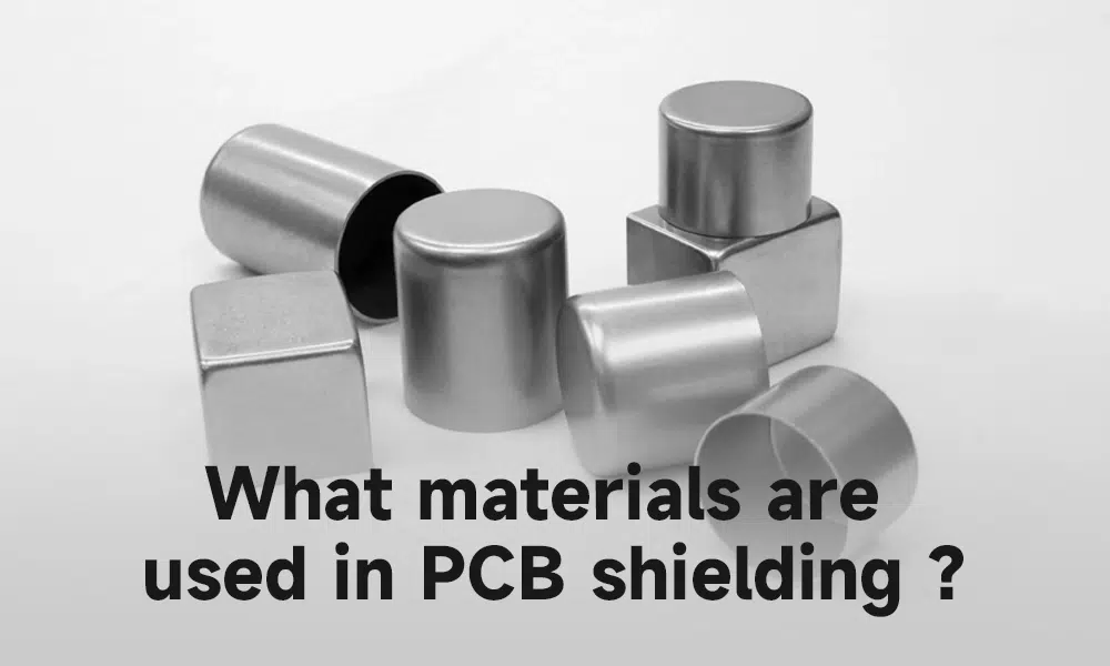
Depending on the required level of shielding efficacy, economic factors, and particular application requirements, several materials can be utilised in PCB shielding. Metals like copper, aluminium, and steel are among the often utilised materials. These metals are easily accessible and have strong conductivity. Materials like conductive paints, conductive polymers, or conductive textiles can be used to create conductive coatings or films. Conductive foams, conductive tapes, and conductive gaskets are additional materials used for shielding.
The selection of material is influenced by a number of variables, including the necessary level of shielding, weight restrictions, simplicity of application, and compatibility with other parts or materials used in the system.
Various methods can be used to protect a PCB from electromagnetic interference (EMI).
First, it’s critical to minimise electromagnetic field coupling between delicate components or lines while designing the PCB layout design. This may be done by isolating analogue signals from high-speed digital signals, reducing the number of signal pathways, and using the right grounding procedures. Crosstalk and interference can be minimised by using ground planes and power planes as barriers between various signal layers.
To further reduce undesirable electromagnetic noise, input and output lines might be equipped with EMI filters. These filters are intended to block or suppress particular EMI-related frequency bands. Utilising shielding materials, such as conductive foils or coatings, over certain components or regions that are especially vulnerable to EMI is another successful strategy. To effectively shield against electromagnetic radiation, these shielding materials must be correctly grounded. In order to guarantee that the PCB satisfies the necessary criteria of electromagnetic compatibility, it is also crucial to comply with pertinent EMI standards and laws.