blogs
Qtech Technology Co., Ltd
SMT / DIP / PCB assembly /
Testing / BGA reworking
QUOTE
close
SMT / DIP / PCB assembly /
Testing / BGA reworking

Attempt to envision a future without modern conveniences like the cell phone, computers, TV, radio, car, and airline. Electronic components can’t be safely attached to devices or connected at their terminals without using a printed circuit board (PCB). Almost no electronic gadget would work without a well-designed PCB layout.
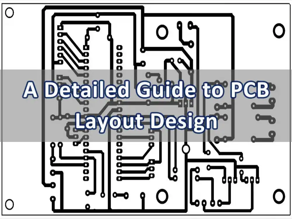
The term “layout” often refers to arranging a product’s components. As such, PCB layout is an umbrella word for several interrelated tasks involved in PCB design. Tracing, mounting completely cutting, labeling, and component placement is part of the process.
Wire routing is a key idea in printed circuit board design. Software developer Autodesk.com puts it this way: “PCB layout design is 90% layout and 10% routing.” When the placement is complete, the next phase is routing. Locating parts on a PCB is part of the placement process. During the routing process, wires link the parts according to the specifications. To make a PCB layout, you may do it by hand or use a computer program. The auto-router function is available in the vast majority of PCB design programs. Many designers use the auto-router feature due to the time and effort it saves.
PCB design’s auto-router feature may be quicker to go anywhere, but it isn’t necessarily the best. The reason being it’s not always as exact and symmetric as it ought to be. Using the right settings for automated routing is essential for getting the best possible results since this allows the automatic function to compute the routes accurately.
Error and short-circuit risks may be mitigated with a well-thought-out PCB layout. As technology advances rapidly, PCB layout play an increasingly important part in our everyday lives. These PCBs are ubiquitous, serving as the backbone of every electrical product.
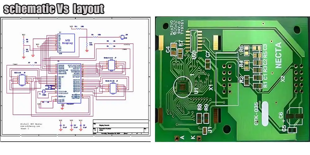
To sum up, the geometry of actual circuits on the PCB is responsible for any discrepancies between the behaviour you discover from simulations using the schematic or your PCB layout. A PCB design is developed into a schematic starting with a circuit diagram. Your PCB layout may be based on this crucial document, which serves as the board’s basis. In a standard 2D CAD assembly design, you’ll depict each circuit and its parts in your schematic diagram.
The printed circuit board design is more complex than it first seems. A well-designed PCB layout will have circuitry physically organised to maximise the board’s electrical performance while maintaining complete manufacturability. This requires careful administration of library components, CAD configurations and settings, component location, trace routing, and power distribution system planning (PDN). To add to this, designers of layouts need to make sure their efforts are well documented and that the end output is ready to be integrated into the larger electronics system for which it was created.
This is a lot for engineers, particularly those who have never worked with PCB layout. A complete set of electronic circuit layout rules accessible for reference might be helpful for this process. Standards within the industry and the company will determine the design’s specifics, although layout principles are still necessary to aid engineers throughout the board creation process. Here are some recommendations for the PCB layout that you may use as a starting point for your standards in this area.
Use IPC or manufacturer specs for package sizes when constructing libraries for the PCB layout. However, some pieces may have to be modified because of personal, business, or technological requirements. Footprints in RF designs, for instance, could need narrower pad widths than in a traditional digital design. For more information on creating your custom PCB component footprints, read on!

Using one or even more continuous flat plates on an interior layer is often the ideal grounding method for current high-speed systems. This offers the highest level of EMI shielding and guarantees unobstructed signal routes, both of which enhance the quality of the sent signal.
You should avoid routing traces through such places if the ground plane is split up on your board because of unusual shapes or features. Your design might generate a lot of extra noise if the signals do not have a continuous and contiguous ground plane to utilise as a clean return channel. Some rules to follow regarding power and ground planes are as follows:

PROTEL Nearly every single circuit company has used PROTEL in some capacity, and several colleges provide courses tailored to its application.
ORCAD is an early example of electronic design automation (EDA) software, dating back to the company’s founding in the 1980s. It has been around as long as Protel, but it’s much worse. ORCAD, on the other hand, has a robust simulation function, a simple user interface, and widespread recognition because of these features.
To meet the ever-shrinking requirements for printed circuit boards, designers are increasingly turning to components with lower footprints and shrinking the space between them. Connectivity and regulation compliance problems may arise from a poorly planned layout.
There is a distinction between a landing pattern and a footprint that is frequently overlooked despite their near-identical names. To be more specific, the landing patterns indicate the pad sizes, and each pad should have an area somewhat bigger than the footprint of the associated component.
When the idea has been finalised, the following step is to develop the circuit diagram. Information like component names, values, ratings, and manufacturer part numbers are included in this diagram to ensure the proper operation of the board’s electrical components.
The component placement follows, which involves deciding where on the board to put each part. It’s not uncommon to go through several iterations of component location refinement.