blogs
Qtech Technology Co., Ltd
SMT / DIP / PCB assembly /
Testing / BGA reworking
QUOTE
close
SMT / DIP / PCB assembly /
Testing / BGA reworking

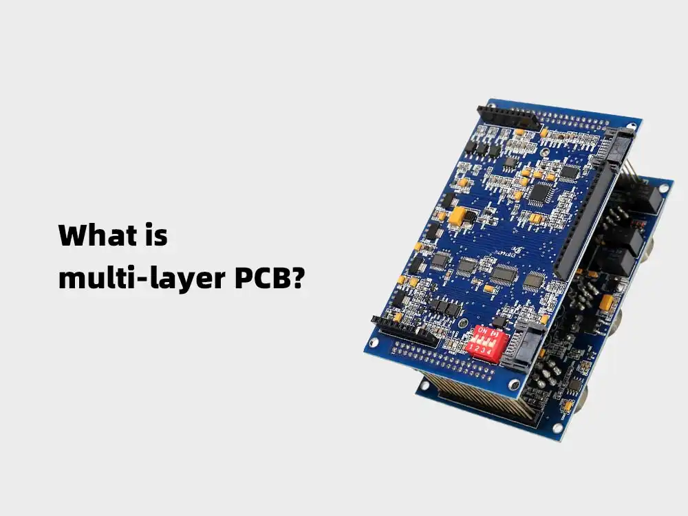
Multi-layer PCB is smartly packed, thin and small printed circuit board, having multiple layers of copper traces and planes on each side of the board. This type of PCB is used for power distribution as it allows for more efficient routing of power voltages between different parts of the board.
If you want to know more about multi-layer PCBs, their benefits/drawbacks, applications, and differences, this article is for you!
Multi-layer PCB is a way of stacking up multiple layers of copper to create a more dense and stable circuit board.
By looking into it we found, it consists of multiple layers of copper foil laminated onto the substrate. This is done so that it provides a more reliable connection between the chips and components on the board.
Based on the intact structure that makes it durable and powerful to use in electronic circuits, it can also be used in other fields like medical devices, transportation systems, and industrial equipment.
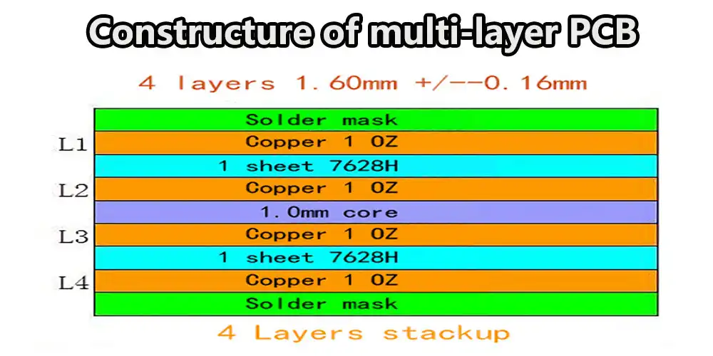
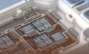
The structure of multi-layer PCB seems a bit more complex than the rest of PCB types. But in actuality, it is pretty understandable.
To enhance electrical conductivity, the layers in a multi-layer PCB are usually made of copper in a repeated way. Fibreglass, paper, or plastic insulating layers separate these copper layers, however, other insulating types can also be used
It is possible to have any number of layers (above 3) in a multi-layer PCB, but the most common type has four or six layers. Typically, four layers are used on a PCB: two for power and two for signal. In a six-layer PCB, four layers are used for power and signal, and two layers are used for ground.
These different models of multi-layer PCB make it suitable for different, heavy-duty tasks in electric circuits, described in the applications section below in this article.
| Difference in Features | Single-layer PCB | Double-layer PCB | Multi-layer PCB |
| Composition: | A copper-based conductive material usually made up of a single layer | Two layers of conductive material should be present | There are three or more layers on a multi-layer PCB |
| Thickness: | Generally thicker than double- and multi-layer PCBs | Thinner than single-layer PCBs but thicker than multi-layer PCBs | Thinnest of the three types because they have the most layers packed into a small area |
| Effectivity: | Least effective at handling high-density and high-speed circuits | Offer more routing space and are more effective | Gives most routing space and is the most effective at handling high-density and high-speed circuits |
| Usage: | Used in simple circuits or circuits with low density and low-speed requirements | Used in more complex circuits with higher density and speed requirements | Used in the most complex and demanding circuits |
| Cost: | Generally the least expensive to manufacture because they have the fewest layers | More expensive to manufacture than single-layer PCBs | Most expensive to manufacture because they have the most layers and require the most material and labor |
It is used to create circuits with specific electrical characteristics, such as a specific polarity or voltage level, by separating the layers and using them as electrical planes.
It electrically isolates different circuit elements from each other by using insulating layers between the conductive layers. This is useful to prevent electrical interference and improve the overall performance of the circuit.
It’s being used in alarm systems and surveillance cameras, to protect against tampering and improve the reliability of the system.
Protect circuit elements from mechanical damage by enclosing them within the PCB layers. This can help improve the overall durability and reliability of the device.
Step 1: Layout and design of a PCB sheet
Using computer-aided design (CAD) software, the layout and design of the PCB are created and verified for accuracy and manufacturability.
Step 2: PCB sheet manufacturing
Then comes the photolithographic process, where a photomask with the desired circuit pattern is transferred onto a photosensitive material on the PCB substrate.
Step 3: Burn-in process of the substrate
Next, it is heated to a high temperature in order to harden and strengthen the material.
Step 4: Fabrication of the circuit layer
The circuit layer is then fabricated by applying a layer of conductive material, such as copper, to the surface of the substrate and etching away the excess to create the desired circuit pattern.
Step 5: Burn-in process of the circuit layer
It is done as it helps to ensure the integrity and reliability of the connections between the various components on the PCB.
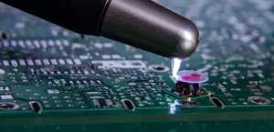
Step 6: Assembly
Finally, the various components, such as capacitors, resistors, and integrated circuits, are placed onto the PCB and soldered into place to complete the assembly.
1. Solder mask delaminates from the copper layer underneath it,
Solution: Use more flux when applying the solder mask to ensure good adhesion, apply heat slowly, and use a non-hardening flux.
2. Flux can be applied too heavily and cause solder balls to form on the surface of the board
Solution: Reduce flux strength or switch to a low-melting point flux (such as lead-free solder) to prevent solder balls from forming on your boards.