blogs
Qtech Technology Co., Ltd
SMT / DIP / PCB assembly /
Testing / BGA reworking
QUOTE
close
SMT / DIP / PCB assembly /
Testing / BGA reworking

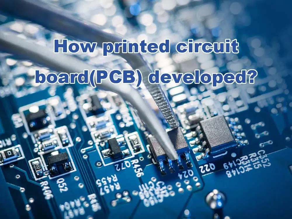
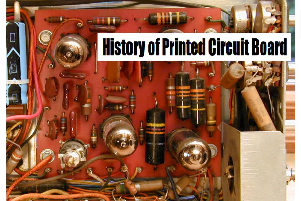
The development of printed circuit boards, or PCBs, has a rich history dating back to the early 20th century. PCBs were originally created as a solution to the complex wiring systems found in early electronics, and over time have become a critical component in the manufacturing of electronic devices. Let’s see how printed circuit board(PCB) developed!
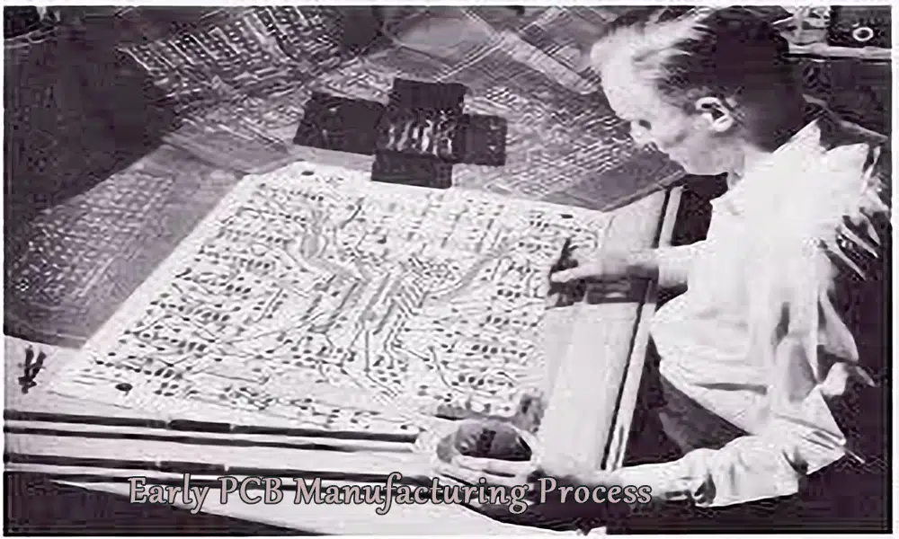
A printed circuit board was born in Japan in 1936. But the work that really gave it significance was done by Dr. Eisler in England. In 1940, with the help of mature processes such as photography, plate making, and corrosion in printing technology, he manufactured the first printed circuit board with practical value on an insulating substrate covered with metal foil.
In 1947, the United States held the first printed circuit technology seminar, which summarized the main manufacturing methods of printed circuits before, and summarized them into six categories: coating method, spraying method, molding method, powder pressing method, vacuum coating method and chemical deposition method.
However, these methods have not been able to achieve large-scale industrial production, and some of them are still used for reference and extended. For example, ceramic substrates suitable for coating method to manufacture hybrid circuits have been retained as an important technology, and circuit boards formed by printing conductive paste on insulating substrates have gradually attracted attention and will be promoted to industrialization in the future. In addition, the chemical deposition method is the basis of the additive method to manufacture printed circuit boards, and it is still under research and development.
The concept of the “Printed Circuit” was first proposed by Dr. Eisler of the United Kingdom in 1936, but it did not arouse the interest of electronics manufacturers at that time. Dr. Eisler was dissatisfied with the research and comparison of the original process methods, so he proposed the copper foil etching process. It was he who pioneered the current mainstream printed circuit large-scale manufacturing method, that is, after coating the insulating substrate fully covered with metal foil with etching-resistant ink, then corroding the unnecessary metal foil to form a printed circuit board.
In 1942, he used a paper laminated insulating substrate to bond copper foil, screen-printed conductive patterns, and then etched away the unnecessary copper foil to produce a printed circuit board for radio. This craft was neglected in the UK at the time, but it was first accepted by the Americans. In World War II, Americans applied the technology invented by Dr. Eisler to manufacture printed circuit boards, which were used in military electronic devices and achieved great success, which attracted the attention of electronics manufacturers.
By the early 1950s, the copper foil etching method became the most practical printed circuit board manufacturing technology and began to be widely used. Therefore, Dr. Eisler is also known as “the father of printed circuits”.
Since the copper foil etching method became the main method of printed circuit production, printed circuit technology has developed very rapidly, and it has better adapted to the needs of the rapid development of electronic technology. In fact, the development of printed circuits is carried out almost simultaneously with the development of semiconductor devices.
Let’s see how printed circuit board (PCB) technology developed during 70 years from the 1950s to the 2020s.
Around the 1950s, when the transistor came out, a single-layer PCB could meet the application requirements of a transistor radio. Products are mainly civilian appliances, such as radios, televisions and so on.
The manufacturing method of single-layer PCB is to use copper-clad paper-based phenolic resin laminate (PP board) as the base material, and use chemicals to dissolve the unnecessary copper foil on the PP board, and the remaining copper lines are all designed circuits. This production technique is called the “subtractive process”.
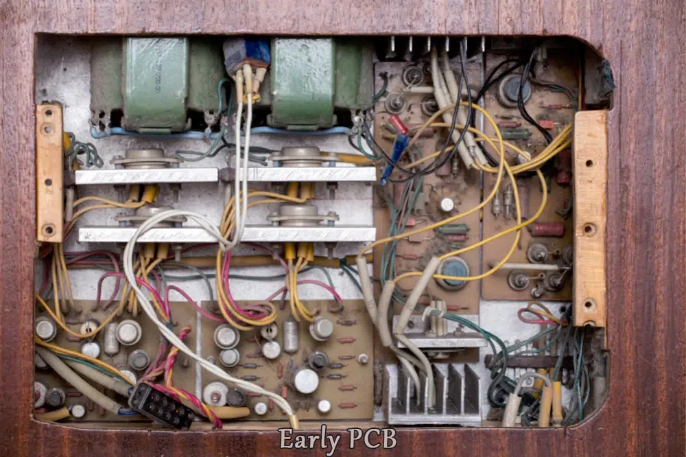
However, even in some branded electronics manufacturers at that time, the PCB subtractive process was still dominated by manual operations, and the corrosive solution used was ferric chloride. At that time, the representative application product of printed circuit boards was Sony’s portable transistor radio, which was a single-sided PCB using PP substrate. In 1958, Japan published the earliest enlightenment book in the printed circuit industry, namely “Printed Circuits”.
In the late 1950s, electronic tubes were gradually replaced by transistors, and the electronics industry entered the “transistor era”. In order to meet the needs of production development, the printed circuit board has developed from a single-sided phenolic resin base to an epoxy resin-based insulating layer material reinforced with glass fiber cloth.
In 1955, Oki Electric Company of Japan entered into technical cooperation with Raytheon Company of the United States to manufacture marine radar. Raytheon Company specifies that the PCB should be applied with copper-clad glass cloth epoxy resin laminate (GE substrate). The GE base material developed in Japan has realized the mass production of marine radar.
Since 1960, OKI Electric Co., Ltd. began to use a large number of GE substrate materials on the PCB of mass-produced electrical transmission devices. In 1962, the Japan Printed Circuit Industry Association was established. In 1964, the American Optical Circuit Company developed a thick copper electroless copper plating solution (CC-4 solution), and started a new additive process for manufacturing printed circuit boards. Hitachi Chemical Company introduced CC-4 technology for GE substrate of PCB. In the initial application, GE substrates had problems such as heating warpage and copper foil peeling, which were significantly improved after gradual improvements by material manufacturers. Since 1965, several material manufacturers in Japan have begun to mass-produce GE substrates.
Around 1960, “double-layer PCB” and “hole metallized double-sided printed circuit boards” with circuit patterns on both sides were put into production one after another. At the same time, “multi-layer printed circuit boards” that overlapped several layers of printed circuit boards were also developed. At this time, the products were mainly used in precision electronic instruments and military electronic equipment.
Around 1968, medium and large-scale integrated circuits had been developed and put into production. The “hole metallized double-sided PCB” that is compatible with it has gradually replaced the single-sided PCB, and a soft, foldable and bendable “flexible PCB” has also been developed.
After 1970, the emergence of large-scale integrated circuits accelerated the development of printed circuits in the direction of multilayering. Electronic computers with small size and many functions have also come out one after another. Communication equipment manufacturers such as Japan’s Oki Electric Co., Ltd. have set up PCB production factories, and PCB professional manufacturing companies have also risen rapidly.
At this time, the use of plated-through holes to realize the interlayer interconnection of PCB is gradually adopted. In the 10 years from 1972 to 1981, the amount of PCB production in Japan increased by about 6 times (the output value in 1972 was 47.1 billion yen, and the output value in 1981 was 302.1 billion yen), which is a leapfrog record.
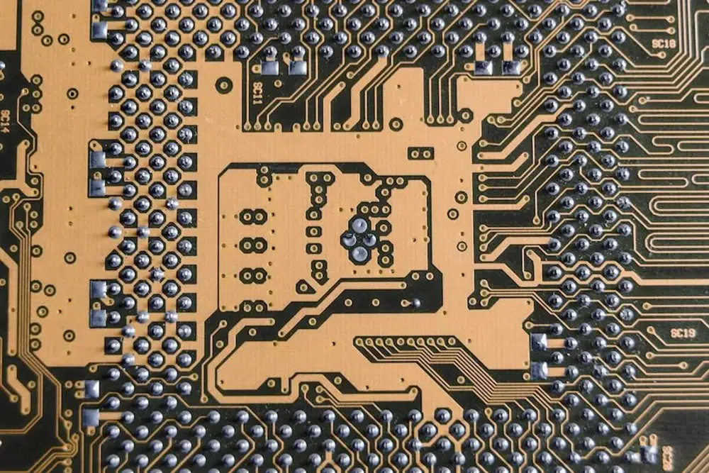
Since 1970, the number of PCB layers for electronic switches of telecommunications companies has reached 3 layers. Since then, the development of large computers has promoted the development of more layers of PCB. The number of layers of PCB also starts from 4 layers to 6, 8, 10, 20, 40, 50 layers, and even more layers. At the same time, PCB also achieves high density (refinement of lines, miniaturization of holes, thinning of insulating layer), and the width and spacing of lines are reduced from 0.5mm to smaller sizes of 0.35mm, 0.2mm, and 0.1mm. This greatly increases the wiring density per unit area of the PCB.
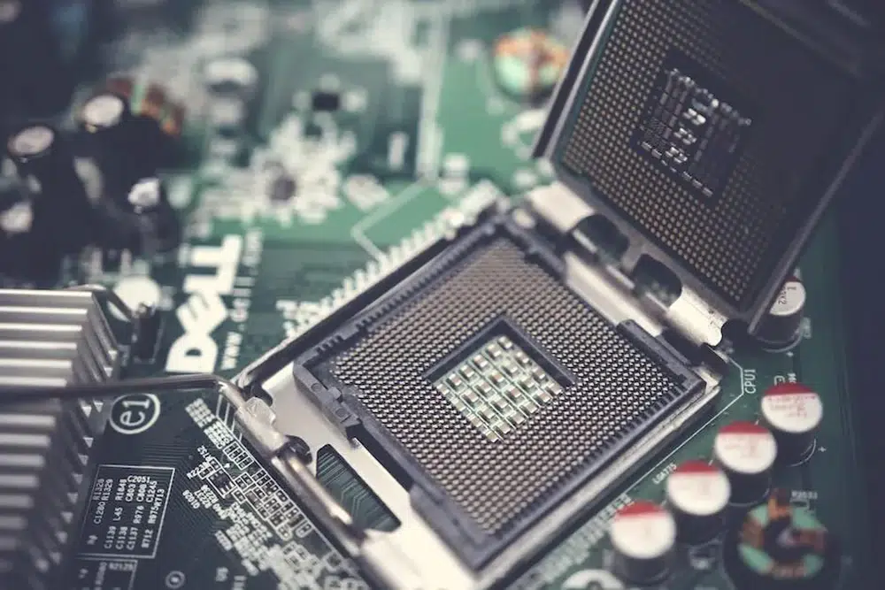
In addition, the installation method of components on the PCB has begun a revolutionary change, and the original Through-hole Mounting Technology (THT) has gradually developed into a more sophisticated surface mounting technology (SMT). Historically, Through-hole Mounting Technology have relied on manual operations on PCBs. The successful development of automatic component insertion machine has realized the automatic assembly of components. SMT uses an automatic assembly line to realize the placement of electronic components on both sides of the PCB.
After 1980, with the development of ultra-large-scale integrated circuits, it was combined with high-density multilayer printed circuits, and supercomputers with hundreds of millions of calculations appeared. In the 10 years from 1982 to 1991, the output value of PCB in Japan increased by about three times (the output value in 1982 was 361.5 billion yen, and in 1991 it was 1,094 billion yen). The output value of MLB was 146.8 billion yen in 1986, which exceeded the output value of single-sided PCB; by 1989, it was 278.4 billion yen, which was close to the output value of double-sided PCB.
After 1980, the high density of PCB increased significantly. A glass-ceramic-based MLB with up to 62 layers formed. MLB densification has effectively driven intense competition in the development of mobile phones and computers. In 1988, IBM Corporation of the United States took the lead in using up to 42 layers of printed circuits in the production of computers. And now, 80-layer high-density printed circuit has also been put into application.
After 1991, the Japanese bubble economy burst, and electronic equipment and PCBs were greatly affected. Gradually recovered after 1994, MLB and flexible PCB also began to grow rapidly, while the output of single-sided PCB and double-sided PCB began to decline.
Since 1998, the build-up method MLB has entered the practical period, and the output has increased rapidly. At the same time, it promotes the miniaturization and ultra-high-density installation of integrated circuit (IC) packaging in the era of area array termination ball grid array (BGA) and chip scale packaging (CSP). With the large-scale development of chip components, SMT technology has entered a period of rapid development in this era, which has significantly increased the interconnection density of electronic products.
With the development of electronic products in the direction of miniaturization and thinning, especially the emergence of smart products and equipment, the mounting area of printed circuit board surface components is greatly limited. The three-dimensional installation of components or IC devices, that is, the integrated integration of PCB has become the most important technology in the manufacture of printed circuit boards in the 21st century. For now, the embedding of electronic components can reduce the area of printed circuit boards by 40%, which can greatly reduce the size of printed circuit boards and give more area to batteries or other components.
Over the past 70 years, the development of PCB has changed greatly. Since the invention of semiconductor transistors in 1947, the form of electronic equipment has undergone great changes. Semiconductors have developed from integrated circuits (IC), large-scale integrated circuits (LSI), and very large-scale integrated circuits (VLSI) to high integration.
More integrated IC package methods such as multi-chip modules (MCM), ball grid arrays (BGA), and chip-scale packaging (CSP) have been developed. The research on printed circuit board technology in the early 21st century will continue to strive for the realization of high density, miniaturization, light weight and high integration of electronic products, and the leading innovative technology “nanotechnology” in the 21st century will also promote printed circuit products and technology development.