blogs
Qtech Technology Co., Ltd
SMT / DIP / PCB assembly /
Testing / BGA reworking
QUOTE
close
SMT / DIP / PCB assembly /
Testing / BGA reworking

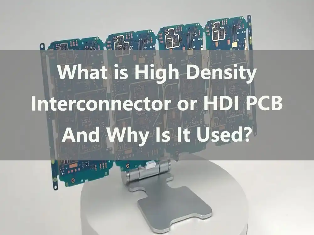
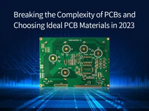
In comparison with traditional PCBs, High Density Interconnector PCB or HDI PCBs provide more components and connections inside a smaller area due to their high density and compact design.
The purpose of this article is to explore the characteristics, benefits, and applications of HDI PCB. We will also discuss the manufacturing process and challenges involved in producing these complex and advanced PCBs. This guide will give you a better understanding of HDI PCBs and how they can be used in various industries.
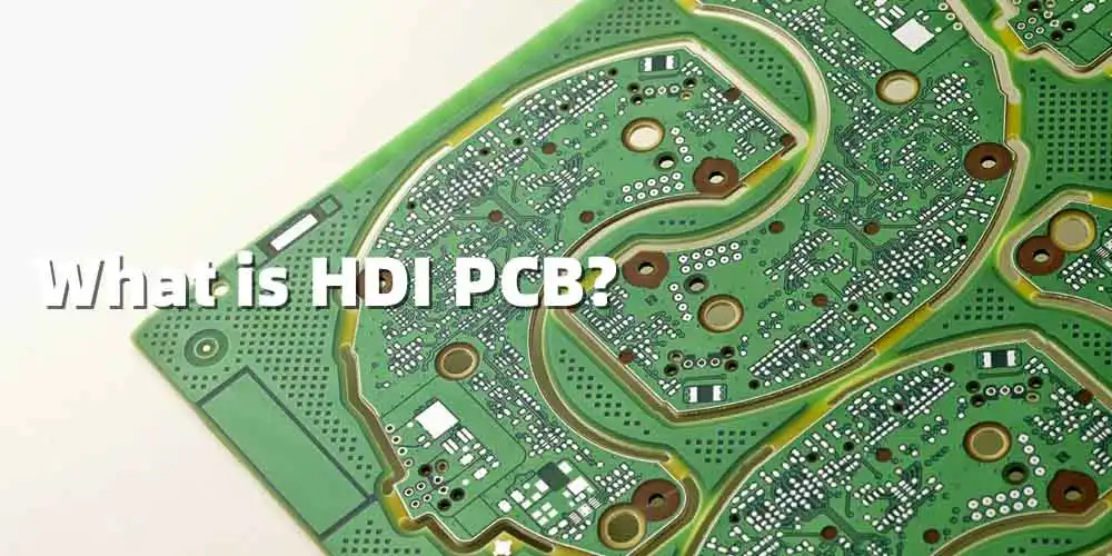
High Density Interconnect or HDI PCB is a type of PCB that utilizes microvias, which are smaller and more densely packed than traditional vias, to connect layers of the PCB and increase the number of interconnections per unit area.
We can also say that it is a multi-layer PCB that uses fine-pitch solder masks, high-density copper tracks (wiring), and advanced materials to maximize performance and minimize cost.
The term “high density” refers to the amount of copper in each layer of the board. A typical HDI PCB has between 140 and 160 layers, which means that there are over 200,000 copper pads on each board. The more layers you have, the more connectivity you can have between
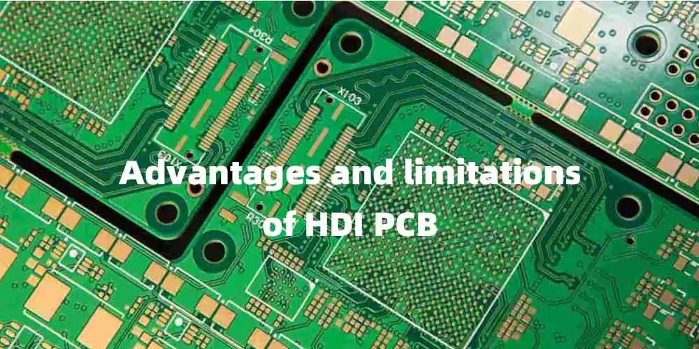
Advantages:
● Higher component density: Smaller trace and spacing widths, allowing for more components to be placed in a smaller area.
● Improved signal integrity: The smaller trace widths and closer spacing of HDI PCBs reduce noise and improve signal integrity.
● Enhanced performance: Lead to better overall performance in electronic devices.
● Increased design flexibility: Designed with multiple layers in a smaller space, allowing for more complex and flexible circuit layouts.
Limitations:
● More expensive to manufacture due to the advanced technology
● More difficult to design and manufacture
● Limited availability as not all manufacturers produce it
The following factors must be considered when selecting HDI PCB material:
You also need to choose between these dielectrics to use in HDI PCB:
| Dielectric | Suitable for: |
| Polyimide | ● High-temperature resistant material● Excellent dimensional stability● Low dielectric constant |
| PTFE (polytetrafluoroethylene) | ● Low-dielectric constant● Excellent electrical properties● Low coefficient of friction |
| LCP (liquid crystal polymer) | ● High-performance● Excellent electrical and mechanical properties● Low dielectric constant and high-temperature resistance |
| Difference in features | HDI PCB | Standard PCB |
| Structure | Defined by their high-density interconnections and made with a thin, high-quality substrate material with multiple layers of wiring | Have interconnections with larger lines and spaces and use a wider range of substrate materials |
| Thickness | Thinner than standard PCBs and thickness ranges from 0.089 mm to 0.25 mm | Comparatively thicker and thickness ranges from 0.25 mm to 1.5 mm |
| Electrical & Thermal Conductivity | Have higher electrical and thermal conductivity but depends on material used | Also have good thermal and electrical conductivity but a bit less than HDI |
| Manufacturing technique | Laser drilling and microvias | Only have mechanical drilling |
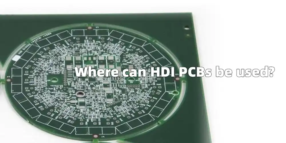
| Usage | High-performance electronic devices that require a high degree of integration and miniaturization, such as smartphones, portable devices, high-end computers or military equipment | Used in standard computers, appliances, and industrial equipment |
| Cost | Generally more expensive | Less expensive than HDI |
PCB design can utilize several types of HDI (high-density interconnect) stack-ups:
| Microvia HDI | Blind/buried via HDI | Sequential build HDI |
| A PCB is connected using microvias (vias with a smaller diameter) | Uses vias that are not visible on the surface of the PCB | PCBs are built in multiple layers with varying interconnect patterns |
| Highly efficient and offer a high density of interconnects | Improve PCB appearance and reduce the risk of interference | High level of design flexibility |
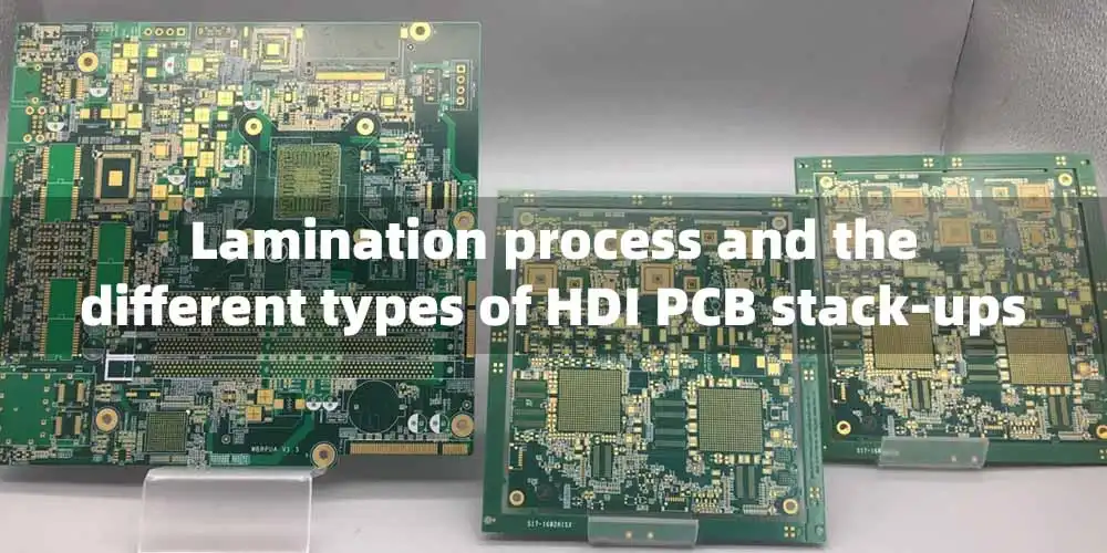
Lamination is the process of bonding multiple layers of material together using heat and pressure. It can be used to create HDI PCBs, which have a higher wiring density and smaller via sizes than traditional PCBs.
● In a microvia stack-up, small vias are used to connect layers of material,
● Through holes in the PCB are used to connect layers without having to pass through the outer layers.
● Rather than bonding all the layers together at once, sequential lamination HDI stack-ups involves adding layers one by one to the PCB.
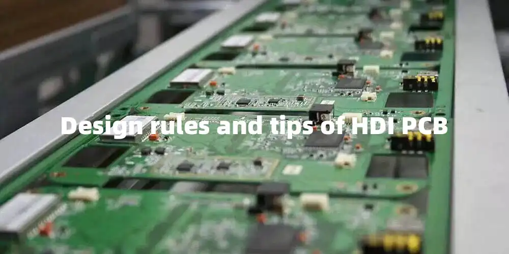
There are several key considerations and design rules to keep in mind when designing an HDI PCB:
● Use small trace and spacing dimensions
● Use high-quality materials
● Consider stack-up carefully
● Choose the right manufacturer
So that’s about everything you need to know about integrated circuits and how they work. We at Qtech are always ready to give you solid advice about PCBs, PCBA, and ICs. Talk to us today and find out more on what we offer. With over a decade of experience in this field, you’re guaranteed quality always.