blogs
Qtech Technology Co., Ltd
SMT / DIP / PCB assembly /
Testing / BGA reworking
QUOTE
close
SMT / DIP / PCB assembly /
Testing / BGA reworking

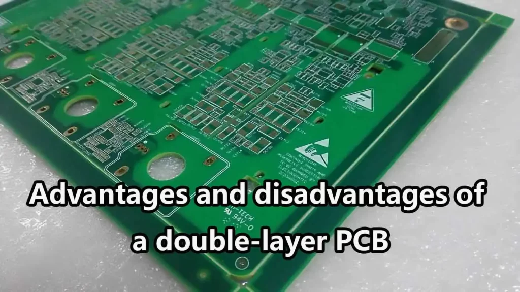
If you’re looking to create a new board for your next project, you’ll want to know all about double-layer PCBs. They’re the latest in PCB technology, and they’re capable of creating boards with a lot more functionality than traditional single-layer PCBs.
But what is a double-layer PCB? And how does it work? In this guide, we’ll answer those questions and more.
PCB stands for printed circuit board and it’s the foundation of many electronics. It provides electrical connections between components on the circuit, including resistors and capacitors.
These connections can be made with a single layer of copper, but when you build more complex circuits, you need to add more layers of copper to accommodate additional connections. When you build a double-layer PCB, you’re stacking two layers of copper together in order to create more complex circuitry.
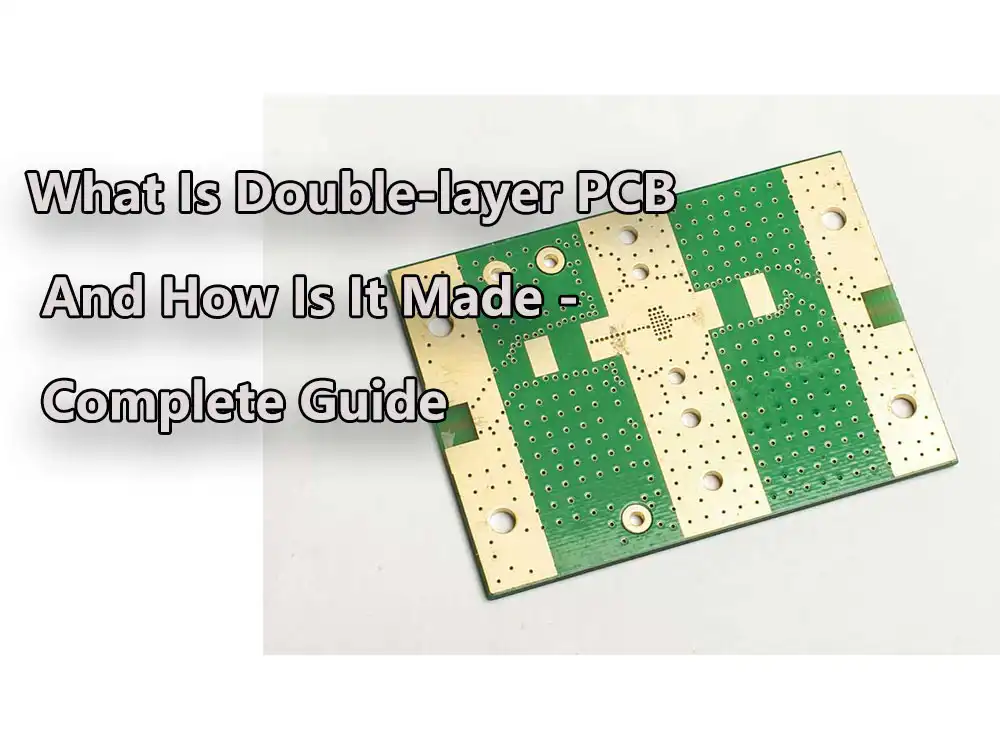
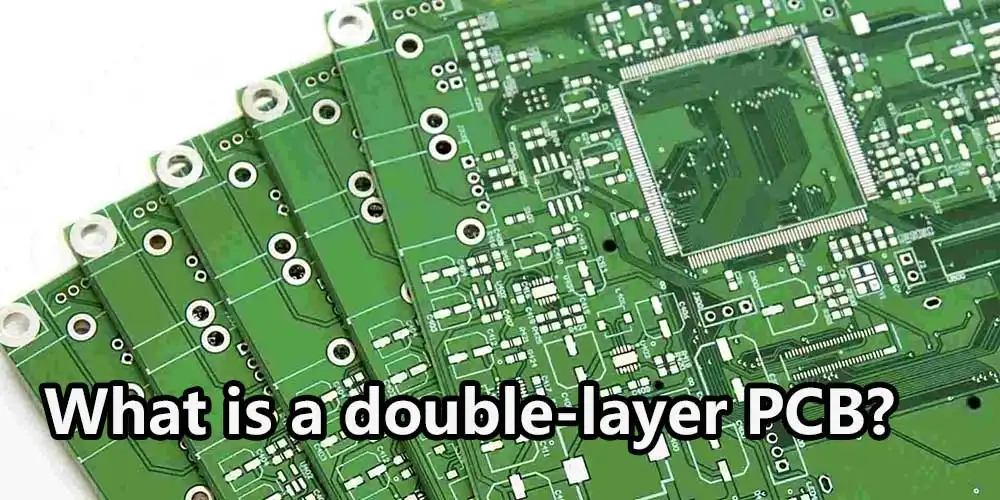
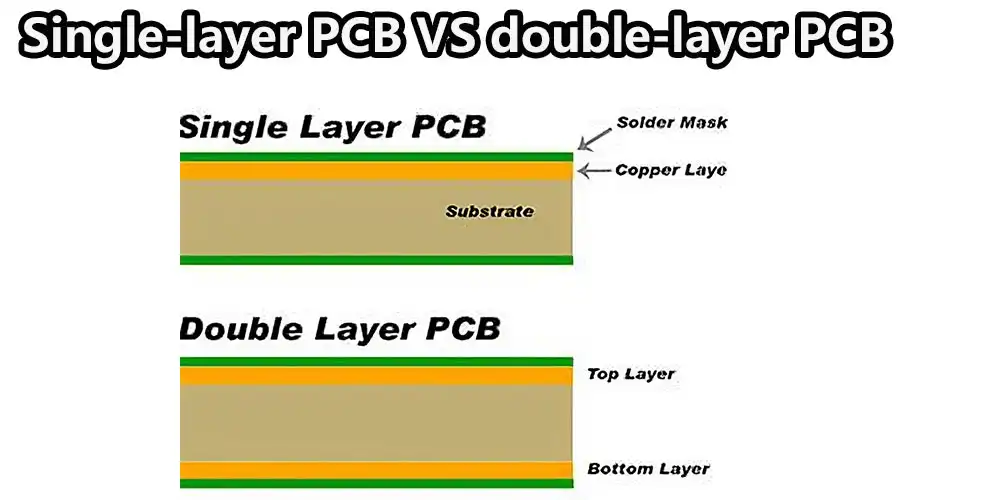
Hence, a double-layer PCB is one that has two copper layers. This is a common technique used in making circuit boards, and it can be used to help reduce the number of connections through the board, as well as increase its flexibility.
A single-layer PCB is the most basic type of circuit board. It can be used in simple applications and has low resistance, but it’s not very durable or reliable. Single-layer PCBs are often used for prototyping and early testing, but they aren’t typically used for production runs.
Double-layer PCBs are just like single-layer PCBs except that they have an extra copper layer, which makes them more durable and resistant to damage. They’re also more reliable than single-layer PCBs because they can carry more current without overheating or breaking down.
In this type, the number of layers depends on how many components you want to fit into your circuit board design and how much current you need to carry through it without overheating or breaking down.
A flexible PCB is a double-layer PCB with a flexible substrate. It is typically used for the production of printed circuit boards that have to be bent, such as automotive components or mobile phones.
● It’s more resistant to heat than a single-layer PCB.
● It’s more resistant to electromagnetic interference than a single-layer PCB.
● It can be used in high-frequency applications.
● It’s easier to route components on it than on a single-layer PCB.
● It has better signal integrity than a single-layer PCB (e.g., resistance to noise and crosstalk).
● The thermal conductivity of the solder mask is lower than that of bare copper, so heat cannot be dissipated as readily.
● Heat will be generated among the copper wires when conducting heavy currents.
● The double-layer PCB is more expensive to manufacture than single-layer PCBs, which Increased time to manufacture.
● More difficult to inspect during the manufacturing process.
| Single-layer PCB | Double-layer PCB |
| The thickness of single-layer PCB is 1oz, which allows it to be cut into small pieces. | The thickness of double-layer PCB is 2oz, which makes it difficult to cut into small pieces and causes the processing cost to increase. |
| ● Single-layer PCBs use only one layer of copper foil as an electrical conductor. | ● Double-layer PCBs use two layers and are therefore more expensive than single-layer PCBs. |
| ● Not as effective as double-layer PCB in grounding capabilities | ● Better grounding capabilities |
| ● Normal conductivity | ● More reliable conductivity |
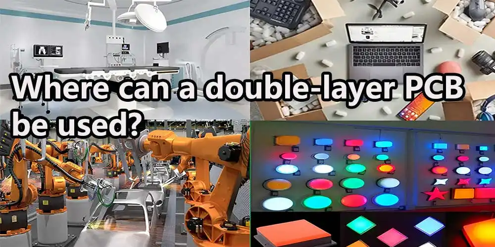
Double-layer PCBs are used in a variety of applications because they provide increased performance and reliability. They can also help reduce the number of components needed, which can translate into cost savings. Some examples include:
Double-layer PCBs are perfect for power supplies because they allow for high current along with high voltage. These circuit boards are also very reliable and durable.
Double-layer PCBs help make telecommunications equipment more efficient by reducing energy losses through heat dissipation. This means that your phone won’t get hot while you’re talking on it!
They also have excellent electrical conductivity, making them ideal for use in sensitive environments like hospitals or laboratories where there may be dangerous electromagnetic interference present as well as high voltage surges that could cause damage to standard circuit boards (such as those found inside computers).
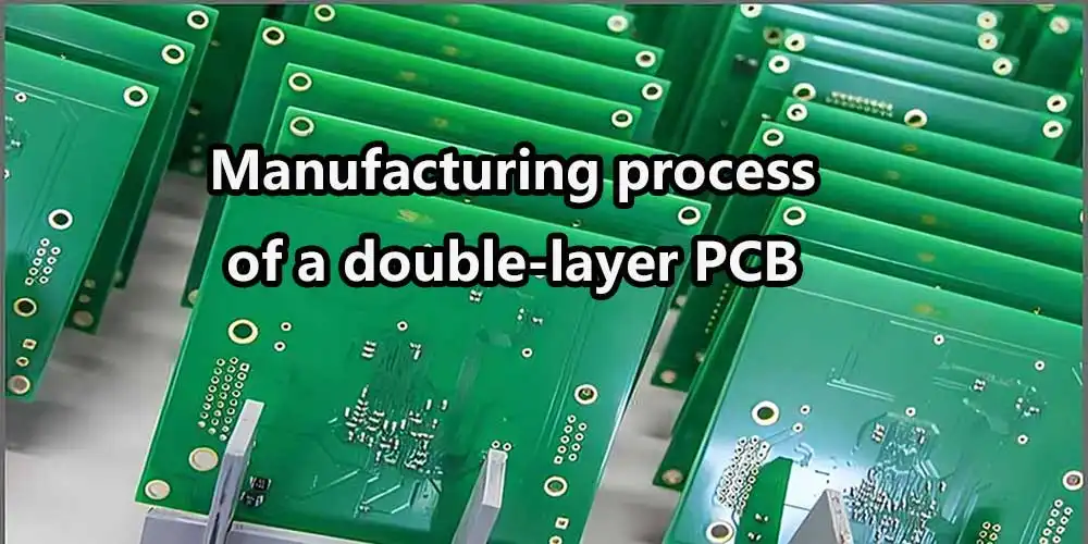
The manufacturing process of a double-layer PCB starts with the creation of the two layers.
The first layer is created using photolithography and etching, while the second layer is created using electroplating to form a thin layer of copper over the entire surface. The thicknesses of these layers vary depending on their purpose in the circuit board.
After all components have been soldered on both sides, the boards are cleaned and inspected for defects before being packaged and shipped to customers who will use them in their products!
The surface of the PCB should be smooth, flat, and free of scratches and nicks. If there are any scratches or nicks on the surface, they need to be removed before they are etched.
The solder mask should be free of scratches and nicks, otherwise it may not be possible to solder components onto the PCB once it is etched. It is important that there are no gaps in the solder mask where components can be soldered through them.
The thickness of the copper should be uniform across all layers of the PCB, but if this isn’t possible because of design constraints then at least make sure that one layer isn’t significantly thinner than another layer (less than 2% difference).
When designing a double-layer PCB, there are a few things to keep in mind:
– The first is that the top layer should be the highest quality layer. It should have the most layers and be printed with a higher resolution.
– The second thing you need to consider when designing a double-layer PCB is how much space you want between each layer.
– Another thing you’ll want to think about when designing your double-layer PCB is whether or not you want a ground plane on both sides of the board, or just one side of it (or neither).
So that’s about everything you need to know about integrated circuits and how they work. We at Qtech are always ready to give you solid advice about PCBs, PCBA, and ICs. Talk to us today and find out more on what we offer. With over a decade of experience in this field, you’re guaranteed quality always.