blogs
Qtech Technology Co., Ltd
SMT / DIP / PCB assembly /
Testing / BGA reworking
QUOTE
close
SMT / DIP / PCB assembly /
Testing / BGA reworking

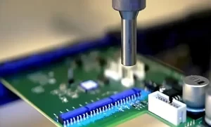
Soldering is one of the most important processes in PCBA processing. On printed circuit boards, electrical connections to all components are made via PCB pad. The pads are a very critical part of the PCB that determines where components are soldered on the PCB. The size, shape, and position of pads in a PCB directly depend on the manufacturing quality of the board. Today we will take a look at the PCB pad in SMT(surface mount technology) soldering.
PCB pads, the basic part of surface mount assembly, are used to form the land pattern of the circuit board, that is, a combination of pads designed for special component types. PCB pads are used for electrical connections, components fixation, or both partial conductive patterns. In simple terms, a PCB pad refers to the lead holes on the PCB board and the surrounding copper skin (copper foil) of different shapes.
There are two types of pads in the board: non-via pads, which are mainly used for surface mounted components and devices, and via pads, which are used for in-line components.
The shape of the pad is different, common are square pads, round pads, oval pads, etc., in addition, there are some special pads that are not common, such as teardrop pads, cross pads, etc..
1. Square pad
2. Round pad
3. Island pad
4. Polygonal pads
5. Oval pad
6. Open-shaped pad
7 Plum pad
8. Cross pad
9.Teardrop pad
It consists of the following parts: top solder paste, top solder mask, top copper pad, plane layer connected to padst6ack plating with a thermal, inner copper pad, plane layer insolated from padstack plating, plated through hole, bottom copper pad, bottom soldermask, and bottom solder paste.

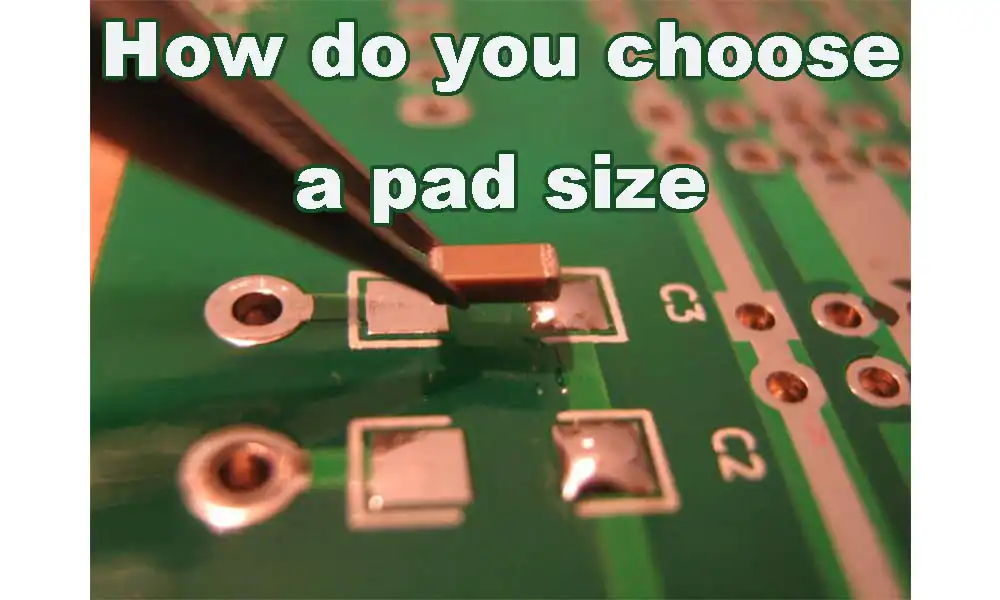
The diameter or minimum width of the single-sided pad is 1.6mm; Double panel weak current line pad only need to add 0.5mm hole diameter, the pad is too large to cause unnecessary continuous welding, the hole diameter of more than 1.2mm or pad diameter of more than 3.0mm pads should be designed as special shape pads.
The inner hole of the pad is generally not less than 0.6mm, because the hole less than 0.6mm is not easy to process when punching, usually the metal pin diameter value plus 0.2mm as the pad inner hole diameter.
The width of the pad should be equal to or slightly larger (or smaller) than the width of the solder terminal (or pin).
(1) Aperture size:
If the actual pin is round: aperture size (diameter) = actual pin diameter + 0.2~0.3mm (8~12mil) or so;
If the actual size is rectangular: aperture size (diameter) = actual pin diagonal size 0.1mm~0.2mm (4~8);
(2) Pad size: conventional pad size = aperture size (diameter) + 0.5mm (20mil).
(3) Processing of via size: the minimum inner diameter of multi-layer board is 0.2mm, the minimum outer diameter is 0.45mm; the minimum inner diameter of double panel is 0.3mm, and the minimum outer diameter is 0.6mm;
(4) The edge spacing from pad to board: >5mil;
(5) Minimum number of characters: line width 6mil, character height 32mil;
(6)Line width / line spacing 4mil/4mil
The formula is as follows:
Pad length B=T+b1+b2
The pad inner spacing G=L-2T-2b1
Pad width A=W+K
The outer pad spacing D=G+2B.
Where: L – component length (or distance between the outside of the device pins);
W – component width (or device pin width);
H – component thickness (or device pin thickness);
B1 – the extension length of the inside (pad) of the solder end (or pin);
b2 – the extension length of the outer side (pad) of the solder end (or pin);
K – The amount of pad width correction.
The distance between pads should be determined based on the size of the component pins inserted (or attached) in the pads, and the corresponding components packaging should be found.
For space of pad mounting hole, the span design has different requirements according to different components, mainly divided into two situations:
For axial components (such as plug-in resistors), for axial components with a pin diameter of less than 0.8mm, the mounting hole spacing is generally more than 4mm longer than the standard hole spacing of the component body.
For axial components (such as plug-in resistors), for axial components with a pin diameter of more than 0.8mm, the mounting hole spacing is generally more than 6mm longer than the standard hole spacing of the component body.
Standard space of pad mounting hole includes: 2.0mm, 2.5mm, 3.5mm, 5.0mm, 7.5mm, 10.0mm, 12.5mm, 15.0mm, 17.5mm, 20.0mm, 22.5mm, 25.0mm, 2.5mm, 5.0mm and 10.0mm hole pitch is preferred.
For radial components, such as plug-in electrolytic capacitors, the mounting hole spacing should match the component pin spacing.

1. Cut off the fallen pad with a knife to the unfallen place to prevent the circuit from expanding along the falling place.
If your component pins are long enough, you can scrape off the insulating paint at the cut circuit connectors, and solder the far-sighted pins here.
If your component pins are not long enough, you can use a thin wire of good solder through the pad holes and solder to the component pins, and the other end to the pad connector and fix it with hot melt adhesive to prevent the solder from falling off again.
2.If the pad falls off very seriously and is not suitable for the above method, you can also choose the way of flying wire, the wire is soldered on the desoldered component pin, the other end is soldered on any solder point connected to the desoldered pad.
3.Bridge. If there are components on the same line around the desoldered pad component pin, you can directly solder the component pin on the pin of that component, abandon the original pad, of course, when soldering, you must see clearly that the string position can not be soldered to prevent burning out the component.
4. Scrape off the green oil on the trace connected to the pad (not too close to the pad, not good to weld the wire), then solder that component, and use the wire to directly connect the place you scraped to the pin of the component.
In PCB layout design, both vias and pads can perform similar functions. . However, in PCB manufacturing, they are not the same.

● Different effects:
Vias, mainly play the role of electrical connection. The pads not only play the role of electrical connection, but also play the role of mechanical fixation.
● Different surface treatments:
The via surface can be coated with or without solder mask. There must be no solder mask ink on the surface of the pad, because this will affect the soldering, and PCB flux must be added in PCB pad.
● Different sizes:
The aperture of VIA is generally small, and usually as long as the plate processing process can do it. The aperture of the pad must be large enough to pass through the pins of the component.
● The minimum width:
The minimum width of the vias is 0.15 mm (under the general process) to ensure reliable copper plating. The minimum width of the solder ring of the pad is 0.20mm (in the case of a common process) to ensure the adhesion of the pad.
In the soldering process used for PCB assembly, using incorrectly sized or incorrectly positioned pads can lead to many problems.
● Floating parts: If surface mount parts are on pads that are too large or not properly spaced, parts may float into wrong place during reflow.
● Incomplete solder joints: Pads that are too small or spaced too close may not leave enough space to form sufficient solder feet. This may result in poor weld connections of the part or no solder joints at all.
● Solder bridging: As mentioned above, an excessively large surface mount pad can float the part, resulting in solder bridging.
Tombstone cracking: The extension length of the pad has a suitable range, and too short or too long is prone to Tombstone effect.
● Solder wicking: The wetting force between the solder and the pin is much greater than the wetting force between the solder and the pad, resulting in wicking
● Drill breakout: If a drill hole with too small a pad size is used, the drill bit can drift slightly during normal drilling operations, breaking the pad shape.