blogs
Qtech Technology Co., Ltd
SMT / DIP / PCB assembly /
Testing / BGA reworking
QUOTE
close
SMT / DIP / PCB assembly /
Testing / BGA reworking

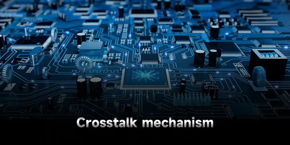
PCB crosstalk is a common issue in PCB design that can cause signal distortion, noise, and timing errors. It occurs when the electric or magnetic fields generated by one trace interfere with adjacent traces. To ensure reliable communication and proper functioning of electronic devices, PCB designers must carefully manage PCB crosstalk.
This article will explore the issue of crosstalk in pcb boards in detail, including what is PCB crosstalk and its mechanism, why crosstalk occurs and how to reduce PCB crosstalk.

PCB crosstalk refers to board (PCB) interfere with signals on an adjacent trace. This interference is caused by electromagnetic fields that are generated by the current flowing through the traces. The fields can induce voltages in nearby traces, leading to unwanted noise and distortion in the signals.
The severity of PCB crosstalk is effected by the distance between the PCB traces, the frequency of the signals, and the characteristics of the traces themselves. Therefore, from PCB layout design to PCB manufacturing to PCB assembly, PCB manufacturers should think about how to reduce PCB crosstalk and provide customers with high-quality and high-performance products.
In PCB design, crosstalk refers to the unwanted electromagnetic coupling between adjacent traces on the board. When signals are transmitted through traces, they generate electromagnetic fields that can cause nearby traces to pick up some of the signal’s energy. This interference can result in signal distortion, noise, or other undesirable effects that can degrade the performance of the circuit.
PCB crosstalk can occur in both digital and analog circuits, and can be influenced by factors such as the distance between the traces, their orientation, the frequencies of the signals, and the materials used in the board’s construction. PCB designers and PCB manufacturers must carefully manage crosstalk to ensure that circuits operate as intended and avoid PCB signal integrity issues.
1. Coupling: PCB crosstalk occurs due to the coupling of electromagnetic fields generated by the signals transmitted through adjacent traces. When a signal passes through a trace, it creates an electric field that can induce a voltage in nearby traces, even those that are not directly connected to it. This phenomenon is known as capacitive coupling. The amount of coupling depends on the distance between the traces, their orientation, and the characteristics of the signals themselves. Inductive coupling can also occur when a changing current in one trace induces a voltage in an adjacent trace.
This mechanism is influenced by the distance between the traces, the frequency of the signals, and the orientation of the traces with respect to each other. The result of these coupling mechanisms is that signals on one trace can interfere with signals on adjacent traces, leading to crosstalk and potentially degrading the performance of the circuit. To minimize crosstalk, PCB designers may use techniques such as careful trace routing, ground planes, and shielding to manage the coupling between traces.
2. Signal or line switching: Two parallel lines in the PCB, when one of them has a high-speed signal transmission, generate an alternating magnetic field, after acting on the other line, generates an induced current inside the line. Now the integration of electronic products is getting more and more high, the packaging is getting smaller and smaller, the PCB trace is getting more and more dense, PCB crosstalk is a particularly difficult to predict and control the phenomenon, inevitable, also cannot be eliminated, can only be reduced as far as possible.

The two main types of crosstalk in PCBs are capacitive crosstalk and inductive crosstalk.
Capacitive crosstalk: Capacitive crosstalk occurs when the electric field generated by a signal in one trace induces a voltage in an adjacent trace
Inductive crosstalk: Inductive crosstalk occurs when a changing current in one trace induces a voltage in an adjacent trace.
Both types of crosstalk can cause unwanted interference between signals and degrade the performance of the circuit. PCB designers must carefully manage these types of crosstalk through proper trace routing, spacing, and shielding techniques to ensure reliable communication and proper functioning of the electronic device.
Crosstalk may be the most important influencing factor in high-speed data transmission, and it may cause data transmission loss and transmission errors. So crosstalk is the biggest natural enemy for PCB design and PCB layout.
The effects of crosstalk on PCB can also include signal distortion, noise, and timing errors. Crosstalk can cause unwanted interference between signals, leading to a reduction in the signal-to-noise ratio, which can degrade the performance of the circuit. In digital circuits, crosstalk can cause errors in data transmission and lead to timing violations, while in analog circuits, it can cause
distortion and affect the accuracy of measurements. Managing crosstalk is important to maintain signal integrity and ensure proper functioning of the electronic device.

To reduce crosstalk in PCB design, several techniques can be used, including:
1. Line track spacing and impedance: appropriately increase the spacing between signal paths; reduce the characteristic impedance of the signal path
2. Return path: Use a plane as the return path;
3. Routing design: Optional routing at the strip line layer; use guard routing with short-circuit via at both ends and across the entire line.
4. PCB selection: use a stack with a lower dielectric constant;
5. Package and Connector: Do not share return pins in package and connector
6. Shielding: During PCB design, a shielding layer can be added between sensitive traces to reduce electromagnetic interference and crosstalk.
7. Termination: Adding a termination resistor at the end of the trace can reduce reflections and signal ringing, thereby reducing crosstalk.
8. Signal lines: Sensitive signal lines, such as audio and other analog signals, should be kept away from digital signal lines as far as possible, and should not be paralleled with digital signal lines; key high-speed signal lines should be wrapped with GND as much as possible.
9. PCB crosstalk analysis: Performing crosstalk analysis during the design process can help identify potential crosstalk issues and allow for adjustments to be made to minimize their effects.
By implementing these techniques, PCB designers can reduce crosstalk and maintain signal integrity, ensuring proper functioning of the electronic device.

Calculating crosstalk in a printed circuit board (PCB) can be a complex process that depends on various factors such as trace length, distance between traces, trace width, and signal frequency. One approach to estimating crosstalk is to use a crosstalk calculator, which is a software tool that can simulate the coupling between traces and predict the level of crosstalk based on input parameters.
To use a crosstalk calculator, you typically need to provide the following information:
1. The distance between the traces
2. The trace length
3. The trace width (PCB trace width calculator)
4. The thickness of the dielectric layer between the traces
5. The dielectric constant of the PCB substrate material
6. The signal frequency and edge rate
7. The type of coupling (capacitive or inductive)
Based on this information, the calculator can estimate the amount of crosstalk between the traces and provide guidance on how to minimize it through adjustments such as trace spacing, routing, and termination.
It’s important to note that while crosstalk calculators can provide valuable insights, they are not always accurate, and the actual crosstalk in a PCB can be affected by other factors not accounted for in the calculations. Therefore, it’s essential to use crosstalk calculations as a guide and to perform crosstalk analysis and testing to ensure the proper functioning of the circuit.