blogs
Qtech Technology Co., Ltd
SMT / DIP / PCB assembly /
Testing / BGA reworking
QUOTE
close
SMT / DIP / PCB assembly /
Testing / BGA reworking

PCB design is an integral part of the field of electronic engineering. PCB design is the entire process of creating a printed circuit board (PCB) based on circuit schematics, through collaboration and integration between multiple disciplines and multiple domains, including electrical, mechanical, software, systems, testing, and manufacturing.
PCB design mainly refers to the layout design, which needs to consider the layout of external connections, the optimal layout of internal electronic components, the optimal layout of metal connections and through-holes, electromagnetic protection, heat dissipation and other factors. In this article, we will fully explain what to know about PCB design.
The first and most important part of PCB design is in its relation to daily consumer electronic devices for many, some common words come up related to hardware components and even the Printed Circuit Board (PCB) term.
For people with technical background in PCB design, it is more about perfectly fitting complicated and small devices through nets of small copper routes that make a device comply with its end purpose. The whole concept of PCB design is about bringing a PCB to the real world and creating it with the proper dimensions according to a specific set of standards and regulations. With the aid of the proper software for PCB design, proper PCB component placement and the routes to be made within the PCB to connect and display all the necessary parts for your circuit board design.
The skeleton of the entire electronic board of a major consumer device relies entirely on the proper function of the circuit board, complying to safety rules for the equipment operation and without negative effects on the end user due to the emissions that can be produced by operating that specific component.
Well, PCB design is about fitting all these assertions and revisions to the product, with the functionality and end life of a determined device given the fact of a specific environment for the device and board to endure and work appropriately. PCB design is the art behind the proper functionality of several electromechanical, aerospace, medic and many other kinds of equipment with such characteristics.
There are many types of PCBs which take into consideration flexibility and thickness. For most common PCB design and testing, there are three common methods for creating the board, which includes ironing on glossy paper over a copper board (copper clad plate) and even drawing the circuit by hand with a special ink (mostly printer ink utilized) that can be passed to the copper board, to then be dissolved with appropriate chemicals in order to remove the unwanted copper (this is called transferring) and have the remaining traces for component placement and soldering.
The last method is with the use of laser cutting tools for etching the edges, but it requires special equipment. The precision is way better with this method, but again, this kind of design will be utilized by PCB manufacturers.
It is appropriate to follow a set of recommended steps in the proper order to assure with higher confidence that a PCB design will produce an effective board on the first iteration and reduce the number of board re-spins.
The first stage of effective PCB design proposes an extensive, but not thoroughly revision of adequate components in terms of quality, shelf life and stocking for their utilization on a specific design which will comply to a specific behavior and set of functions. Once they have been selected, it is important to create and review the related schematic for that specific set of components. Therefore, proper simulation of desired behaviors can be done with computer assistance through dedicated simulation software where possible. On this stage, the elaboration of fast prototypes or component breakout board testing is recommended.
The proper simulation and workout results of the PCB design will lead to the board layout design, which again will consider different rules (trace width, component spacing and placement…) to build a compliant PCB. Finally, a verification and validation stage will ensure in pre-production that the idealized and design board can become real through the specific machinery and manufacturing equipment from the PCB manufacturer with standard design compliant rules.
As stated above, after a schematic was generated, it is compiled by the PCB design tool, which creates a database with the components and their connections or electrical nets on the PCB layout design. From there, the routing of the components has to be done either manually or with the aid of an automated routing tool, which is included on most of the PCB design software suites. It is important to follow the rules and compliance recommendations order to have a compliant PCB. As a summary, a layout is the subproduct of a compiled schematic and the routing of the components utilized in the schematic
The art of PCB Design encompasses various topics, essentially, it consists of the PCB schematics and PCB layout. Basically, the PCB design entails the use and placement of the right components and connecting them adequately and as per their specifications to produce the necessary files that enable their manufacturing. All of this must be previously tested and simulated under special requisites and conditions. Failure is also a part of design, so board re-spin and testing is also a factor to consider when designing an electronic device.
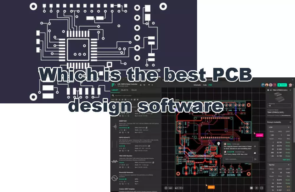
As to which PCB design tool will be the best, the answer could be more related to the skills and abilities of a designer itself as a short answer. However, this does not englobe the total number of applications and plugins that each independent software that there can have. While some software contains a set of features to fully design and simulate a specific circuit, there are also other tools which are focused to specific device design such as automotive components as well as aerospace or special ATE equipment PCBs with high number of layers. As a list for the most recommended PCB design suites, you can find the following:
A.Eagle: It is a software suite provided from Autodesk that allows easy schematic and layout integration, with the possibility of analyzing and visualizing independent layers with a friendly GUI.
B.KiCad EDA: It is one of the trendiest PCB design suites due to its free and open-source origin, it allows to integrate CAD from Eagle and other software and continue the design.
C.OrCAD: The special functions of this design suite is in regard to simulation capabilities. The name stands for Oregon and CAD combination.
D.Altium Designer: It is an evolution of Protel software from the last century. It is one of the most popular and extensive suites due to its complete set of design features and integrations as well as the complete set of component libraries compatible already available.
E.Allegro: One of the most advance PCB design software due to its circuit simulation and measurement integrations.
F.Siemens PADs: This is used for professional and standard automotive industry design as it contains rigid-flex PCB design integrations and analog/mixed simulation specialized for RF circuits.
There are many software tools and suites for PCB design as presented above and they include different plugins that aid in the creation and compilation of both the schematic and PCB layout. However, the PCB designer must take into account some factors for a successful design.
Before creating a schematic, it is important to consider the values, signals, and limitations that the PCB will have (e.g., PCB impedance control, capacitance…). After this, the proper components have to be selected, sometimes they are different from the testing components used on a wired prototype and this is also a standard for beginner designers.
After the component selection and parameter calculation, a schematic will be created. For the PCB layout, it is important to define a proper layer stack-up, which is crucial on high-speed and multilayer PCB design. Then, the routing and component placement will need to be done according to the project related design rules taking into account constraints that are set due to its manufacturability (e.g., minimum via or trace sizes, component spacing…).
Once the PCB design is compliant with the rules and desired connections, the proper manufacturing files (commonly known as Gerber files) have to be generated and provided to a manufacturer. These steps may be repeated according to feedback and PCB design versions.
Any beginner designer should start a design by following these set of basic steps and rules in combination with a series of “thumb rules” provided by standards and previous fabrications to practice and adapt special design criteria.
As your PCB design becomes bigger such as in single board computers or complex power supplies, the probability of failure in the routing, component placement or lack of design considerations is higher. In this case, how is it possible to verify where the problem is and its solution?
First, a particular company and design will intend to have special “thumb rules” as discussed above, which includes width tracing, trace clearance, control of hole and via sizes, as well as clearance between solder masks, all of them attending to a special industry standard as discussed above. PCB design rules are generalizations of creating a PCB abiding to special emissions and protections for the environment and market a special PCB device will be placed.
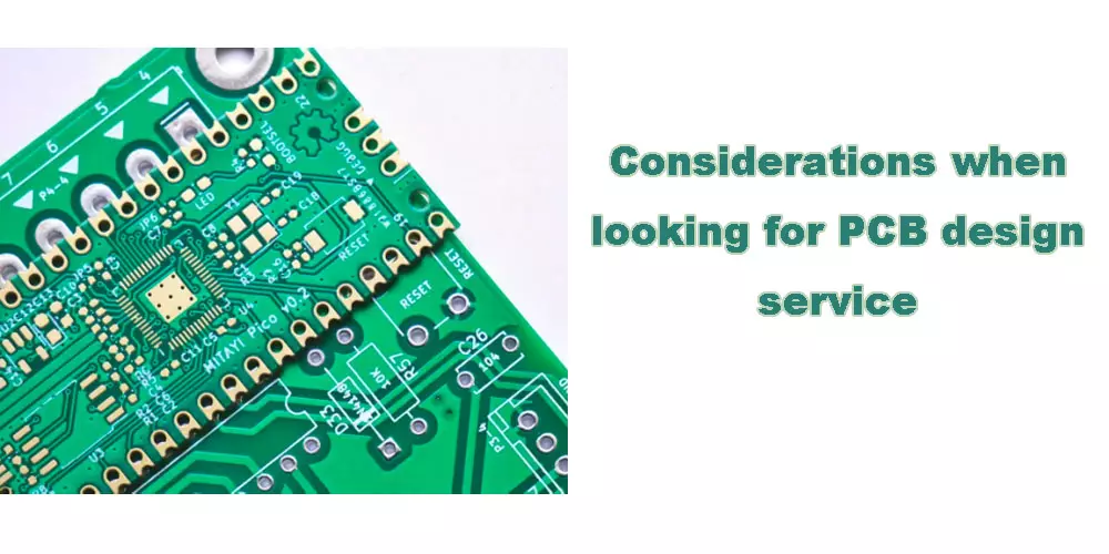
When you bring your PCB design to a manufacturer you must consider a good service partner for your product. Among the most important factors for choosing your PCB manufacturer are reliability, which is the ability to meet specific deadlines, compliance to a set of special requirements, quality and cost efficiency and an added value to the full set of services generally offered by them. Choose the design service that is closer to the pricing and device to be done.
So that’s about everything you need to know about integrated circuits and how they work. We at Qtech are always ready to give you solid advice about PCBs, PCBA, and ICs. Talk to us today and find out more on what we offer. With over a decade of experience in this field, you’re guaranteed quality always.