blogs
Qtech Technology Co., Ltd
SMT / DIP / PCB assembly /
Testing / BGA reworking
QUOTE
close
SMT / DIP / PCB assembly /
Testing / BGA reworking

As a key process in surface mount technology production, reflow soldering is the key to ensure the quality of PCB board and electronics product. Reflow soldering is mainly used to solder the circuit board that has been mounted on the component, melt the solder paste by heating to fuse and solder the patch component and the circuit board pad, and then cool the solder paste through the cooling of reflow soldering to solidify the components and pads together. Improper temperature curve will cause PCB board to have incomplete soldering, missing soldering, component offset, solder balls and other soldering defects, which affecting product quality.
This article will introduce about the definition, technological process, consideration, defects and comparison with wave soldering.
The term “reflow” is used to refer to the fact that the solder alloy is solid but when the temperature is higher than the melting point of the solder, the solder begins to melt and resume flow, hence the term “reflow”.
After one or more electronic components are connected to the contact pad using solder paste (a mixture of solder and flux), the solder is melted by controlled heating to achieve a permanent bond, and soldering can be performed by different heating methods such as a reopening oven, infrared heating lamp or heat gun.
● Advantages of reflow soldering
1. The temperature of reflow oven is easy to control, and oxidation is avoided during soldering.
2. It has a heating circuit inside that heats the nitrogen to a high enough temperature and blows it to the circuit board where the component has been attached, so that the solder on both sides of the component melts and bonds with the motherboard.
3. Dont need to immerse the whole printed circuit board in molten solder, but to complete the soldering task by local heating, so the soldered components are subject to little thermal shock and will not be damaged by overheating.
4. The solder is soldered at the soldering site and with local heating, avoiding welding defects such as bridging.
5. The solder is used once, and there is no reuse, so the solder is pure and has no impurities, ensuring the quality of the solder joint.
● Disadvantages of reflow soldering
Temperature gradients are not easy to grasp (specific temperature ranges for the four operating areas).
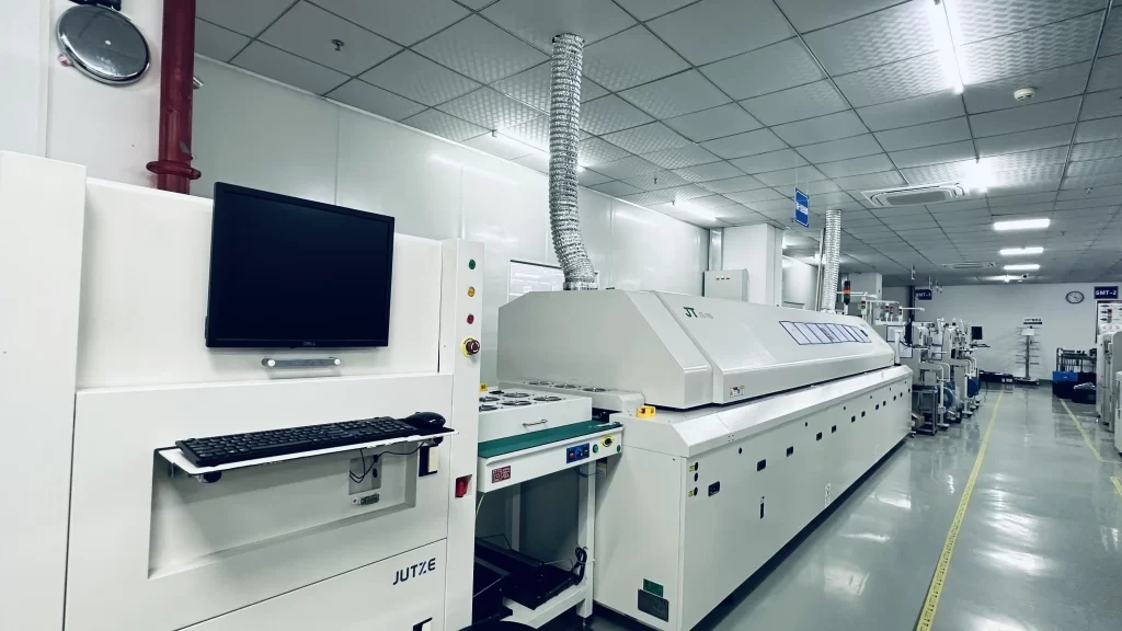
1. Check and make sure that the inside of the equipment keeps clean ( no debris).After confirming cleaning, check the line, ensure safety after booting, select the production program to open the temperature setting.
2. Turn on the air transport, mesh belt transportation, cooling fan.
3. Turn on the temperature zone switch in order, wait for the temperature to rise to the set value, then you can start to pass the PCB. Pay attention to the direction of the board, and ensure that the distance between the two consecutive PCB boards of the conveyor belt is greater than 10mm.
4. The flux in the solder paste wets the pads, component ends, and pins. The solder paste softens, slumps, and then covers the pads, component ends, and pins, isolating them from oxygen.
5. When the PCB enters the insulation area, the PCB and components are fully warmed up to prevent the PCB from suddenly entering the soldering high temperature area and damaging the PCB and eelctronic components.
6. When the PCB enters the soldering area, the temperature rises rapidly to make the solder paste reach the melting state, and the liquid solder wets, diffuses or reflows the pads, component ends and pins of the PCB to form solder joints.
7. The PCB enters the cooling zone to solidify the solder joint. Reflow soldering is completed at this point.
8. Check and electrical test the soldered circuit board, clean and dry it according to the single number, color temperature and voltage classification.
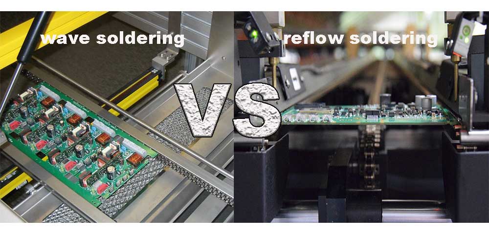
Wave soldering can basically be understood as it only solders for relatively small components, which is different from reflow soldering, and reflow soldering heats the components of the board, in fact, the original brushed solder paste is liquefied, in order to achieve the purpose of connecting the components with the board.
How wave soldering works
The board enters the machine port –> The sensor senses the rear spray FLUX (flux) –> The preheating zone starts to warm –> The tin spray starts to spray –> Cooling.
How reflow soldering works
Several temperature zones are heated -> tin liquefaction –> cooling.
Wave soldering advantages
(1) Its solder is in a flowing state, so that the solder surface of the printed circuit board can fully contact with the solder, and the thermal conductivity is good.
(2) The contact time between the solder and the printed circuit board can be significantly shortened.
(3) The transmission system of the printed circuit board only does linear motion, which is simple to make.
Disadvantages of wave soldering
Solder is sprayed into the air at a very high temperature at a high speed, oxidizing more, and the resulting oxides often cause various forms of soldering defects.
(★ The advantages and disadvantages of reflow soldering are described above.)
Wave soldering is mainly used in perforated or hybrid technology circuit boards, so there is generally a process of cutting off excess wire feet.
Reflow soldering is generally used for SMD packaging, to meet the needs of continuous miniaturization of PCB boards, and is used for SMT technology.
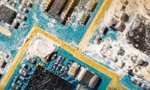
Bridging
Manhattan Effect
Wicking
Poor Wetting(solder joint)
Desoldering
Solder balls
Tin whisker
Offset or reversed (Electronic components)
Flux residue
Pseudo soldering
Missing solder
① It is necessary to understand the quality and soldering requirements on the PCBA, such as high temperature requirements and solder joints and devices that need to be taken care of in terms of life.
② Understand the soldering difficulties on the PCBA, such as the part where the solder paste is printed larger than the pad, and the part with a particularly small spacing.
③ Find out the hot and cold points on the PCBA, and weld the temperature measurement coupling on the point.
④ Determine other places where thermal coupling temperature measurement is necessary, such as BGA package and bottom solder joints, heat-sensitive device body, etc. (try to use all temperature measurement channels to obtain more information).
⑤ Set the initial parameters, and compare and adjust with the process specifications.
⑥ Carefully observe the PCBA after welding under the microscope, observe the shape and surface condition of the solder joint, the degree of wetting, the direction of tin flow, the residue and the solder ball on the PCBA.
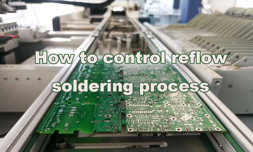
The above six steps are the setting and modulation of the process, and when we are satisfied with its effect, we can enter mass production. Once the welding parameters (temperature, time, air volume, wind speed, load factor, exhaust, etc.) have been determined, it is the goal of process monitoring to ensure that these parameters have some stability.
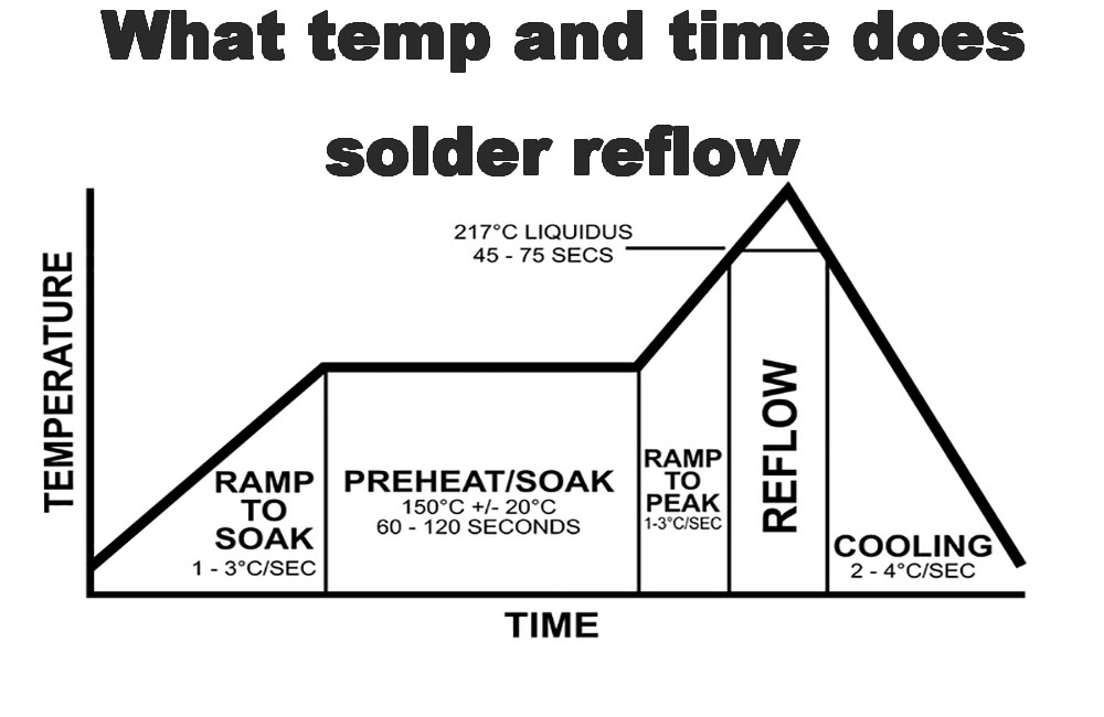
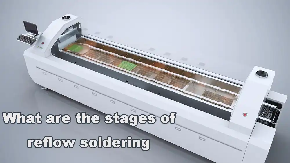
The reflow furnace has 4 zones, which are divided into preheating area, constant temperature zone, tin melting zone and cooling zone.
The heating slope of the preheating zone should be less than 3 °C/sec, and the setting temperature should be ~130 °C at room temperature. The residence time is calculated as follows: let the ambient temperature be 25 °C, if the heating rate is calculated at 3 °C/sec, (150-25)/3 is 42s, if the heating rate is 1.5 °C/s, then (150-25)/1.5 is 85s.
The set temperature of the constant temperature zone is 130°C~160°C, and the constant temperature time is 60~120s.
The heating rate of the reflux zone is controlled at 2.5-3 °C/s, and the peak temperature should generally be reached within 25s-30s.
The cooling rate of the cooling section is generally 3~4 °C/s and can be cooled to 75 °C, and the cooling slope is less than 4 °C/s.
The reliability welding of printed plates, aerospace (QJ) and national military standards (GJB) are not allowed to exceed three times, and it is also strictly stipulated that the process parameters of each welding must not exceed the requirements of the standard specifications. On the one hand, this is based on the fact that multiple soldering will greatly reduce the adhesion (tensile strength) of the printed board pads; On the other hand, multiple welding will also cause poor embrittlement of intermetallic compounds (IMC) in the solder joint, increasing the risk of solder joint breakage. This understanding applies to both leaded and lead-free hot air leveling (HASL) printed boards and chemical nickel-gold (ENIG PCB) printed boards.