blogs
Qtech Technology Co., Ltd
SMT / DIP / PCB assembly /
Testing / BGA reworking
QUOTE
close
SMT / DIP / PCB assembly /
Testing / BGA reworking

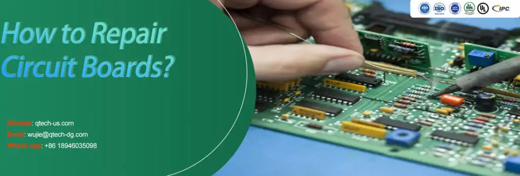
Circuit boards are indispensable components that provide essential power to a vast array of electronic devices. Nevertheless, they are not immune to issues and may experience a range of problems as time passes. In such situations, the decision to repair circuit boards instead of replacing them can offer significant advantages. It is a more cost-effective solution, which also helps in reducing electronic waste and minimizing the environmental impact associated with manufacturing new circuit boards. This guide introduces a step-by-step process for PCB repair, along with an explanation of the causes behind printed circuit board failures and the necessary tools and equipment for successful PCB repair.
Before repairing the circuit board, we need to understand the cause of the failure, which can help us solve the problem faster. Below we list some common causes of PCB failures:
Printed circuit boards contain pathways that facilitate the transmission of signals and power among electronic components. When a PCB sustains physical damage, it can result in operational failure by either disrupting these pathways or causing harm to the components.
For instance, if the board becomes bent or develops cracks, it can lead to the disruption or disconnection of pathways connecting the components. Additionally, excessive vibration or shock can lead to component displacement or detachment from the board, consequently disrupting the circuit’s functionality. Therefore, it is vital to exercise caution when handling and storing PCBs to minimize the risk of physical damage and enhance their longevity.
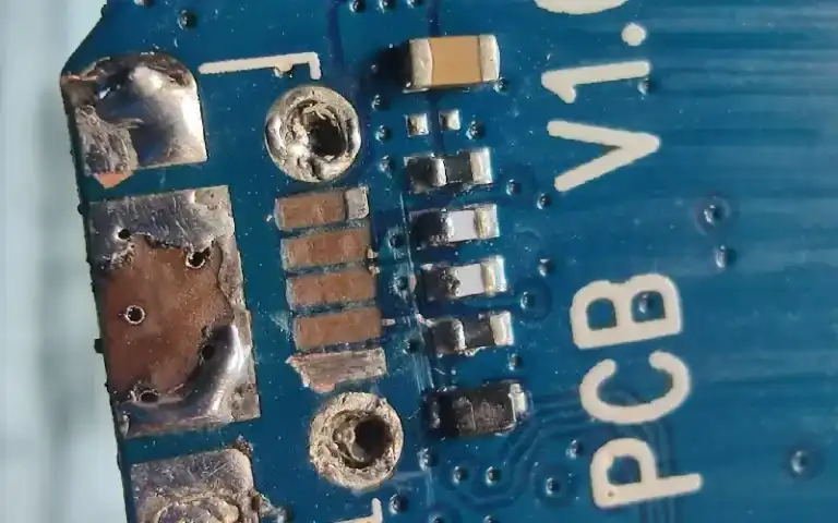
Boards commonly experience component failures, but the advantage is that they don’t impact the physical structure of the board. Over time, the functionality of electronic components may fail due to aging, excessive heat, or electrical faults. Additionally, these individual parts can become loose or disconnected from the board. In such cases, you only need to replace or reattach the affected components using soldering techniques. However, the circuit tracks can be responsible for issues when they lose conductivity due to voltage fluctuations, overheating, or aging. Fixing this problem requires more advanced technical expertise.
Poor PCB design is one of the common causes of PCB failure. A common design fault that can render a PCB non-functional is the improper routing of traces. When traces are not appropriately routed, it can result in signal interference or the creation of high impedance points that disrupt the smooth transmission of signals. For instance, when two traces carrying distinct signals are routed too closely together, they may interfere with one another, causing noise or signal loss. Similarly, if a trace is excessively long or contains numerous bends, it can create a high impedance point, thereby diminishing the strength of the signal. To know more about PCB traces, you can check the blog: The Essential Guide to PCB Traces.
Plating voids pose a potential risk of PCB failures. During the plating process, which creates a conductive layer on the PCB’s surface using materials like copper, small empty spaces or gaps called voids can develop within this layer. These voids can have adverse effects on the PCB’s performance. Incomplete electrical connections or complete circuit breaks can occur due to these voids. Moreover, they can lead to corrosion and deterioration of the PCB over time.
Solder mask delamination occurs when the protective layer on a PCB peels off partially or completely due to mishandling or poor-quality materials. This can affect the board’s appearance and lead to repair issues. Causes include incompatible materials, exposure to moisture, heat, chemicals, and mechanical damage. Preventive measures include using quality materials, proper handling, and storage techniques to ensure the solder mask remains intact and protects the underlying circuitry.
When the etchant solution gets trapped in sharp angles of the board, it creates acid traps that are unable to escape. Consequently, the acid continues to erode the copper, which can result in the breaking of copper traces or pads, ultimately causing a complete failure of the PCB. Therefore, it is crucial to carefully design and inspect the PCB before manufacturing to prevent acid traps.
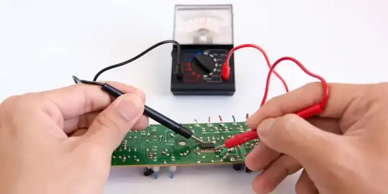
Before commencing the PCB repair, it is crucial to prepare all the tools and materials needed. This proactive step ensures a smooth and uninterrupted repair process. By having everything readily available, you can avoid any unnecessary delays or interruptions.
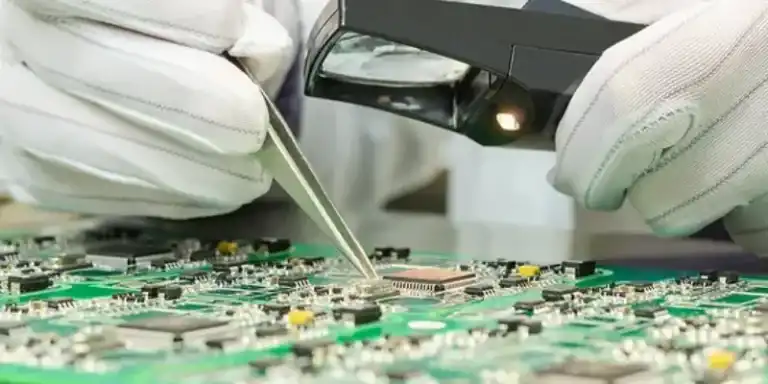
Use a screwdriver or knife to carefully detach the component from the circuit board. This step should be done before attempting to desolder any remaining solder joints. In case the pad is damaged or contains excessive solder, carefully utilize sandpaper to eliminate the undesired material. Exercise caution and avoid applying excessive pressure to prevent any additional damage to the PCB.
It is important to clean the track to ensure proper adhesion and a solid connection for the new component or pad. First, use a cotton swab soaked in rubbing alcohol to eliminate any residue present on the track. Then, employ a craft knife with caution to carefully eliminate any damaged sections of the track. Last, mark the end of the cut track using a pen. This marking will serve as a guide for placing the new component or pad accurately.
Once you have ensured the cleanliness of the track, proceed with placing the copper tape over it. This step is essential to establish a strong connection for the new component or pad. Begin by cutting a piece of copper tape that is slightly longer than the track itself. Carefully position the tape directly over the track, ensuring full coverage. Aligning the ends of the tape precisely with the edges of the circuit board. This ensures a secure and reliable connection for the new component or pad.
Using a soldering gun, apply a small quantity of solder to a pad and heat it until it melts. Next, gently press the tip of the soldering gun against the copper tape, ensuring it remains in position until the solder cools down and creates a strong connection. Repeat this procedure on the remaining pad, makings sure both joints are properly soldered.
Begin by using a sharp knife to remove any debris or obstructions from the hole, ensuring it is clean and free from any dirt or leftover solder. Next, take a cotton swab dipped in rubbing alcohol and carefully clean the through-hole, removing any remaining contaminants. Finally, resize the hole to match the size of the component lead using a paper clip or a similar tool, gradually widening it until it securely accommodates the lead.
To solder the new component onto the PCB, carefully insert its lead into the through-hole for a secure fit. Flip the PCB to access the soldering side, then apply solder to one pad using a soldering gun, melting it for bonding. Connect the lead by touching the soldering gun’s tip to the pad, holding until the solder cools and forms a strong bond. Repeat the process on the other pad, applying solder, heating, and connecting the lead until a secure bond is formed.
The last step to repair circuit boards needs to be done with care. Utilize tools like a craft knife to remove the additional tape surrounding the repair. Be mindful not to cut or damage any of the tracks or pads on the PCB while trimming. This ensures a clean and tidy appearance while maintaining the integrity of the circuitry.
Although it is more cost-effective to repair circuit boards than to buy a new circuit board, it will be a better choice if you buy a high-quality circuit board from the beginning. Hence, working with a top-notch PCB manufacturer is very critical. At Qtech Technology, we take pride in our ability to produce top-notch PCBs and provide exceptional PCB assembly services. With the utilization of cutting-edge equipment and advanced technology, we prioritize quality control throughout our production process. Contact us today to discover how we can assist you with your PCB project.