blogs
Qtech Technology Co., Ltd
SMT / DIP / PCB assembly /
Testing / BGA reworking
QUOTE
close
SMT / DIP / PCB assembly /
Testing / BGA reworking


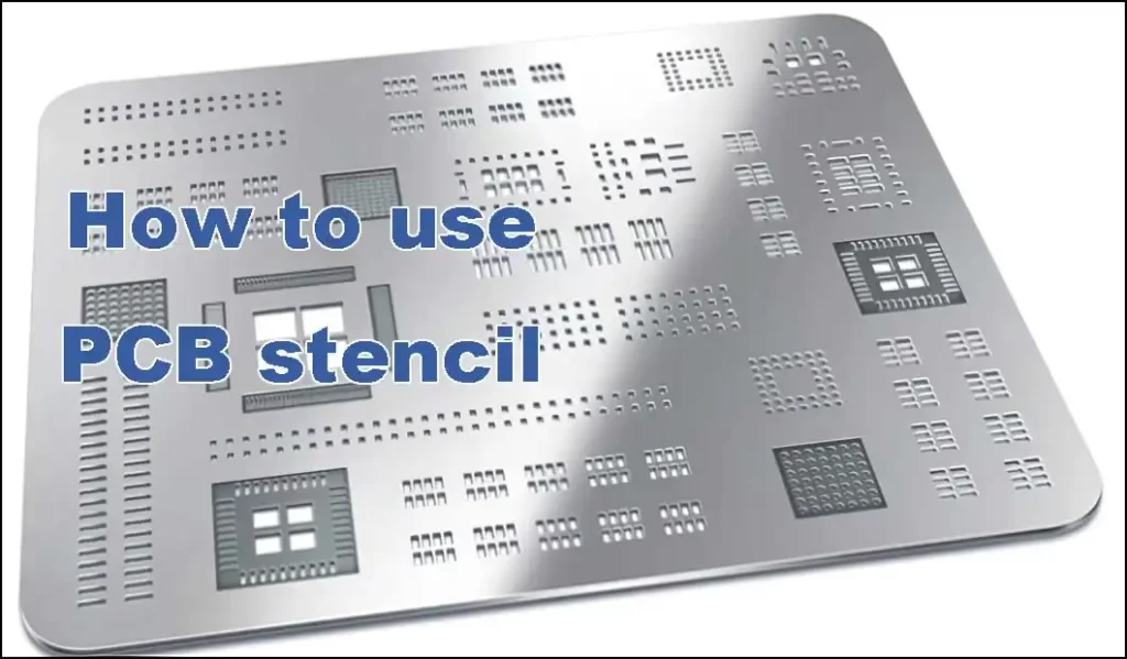
PCB stencils are an essential tool used in the manufacturing of printed circuit boards (PCBs) and PCB assembly. They are thin sheets made of stainless steel or polymer with precision-cut openings that correspond to the pattern of pads and through-holes on a PCB. PCB stencils help ensure accurate and consistent placement of solder paste on a PCB. PCB stencils are made to be reused multiple times. However, how long a stencil lasts depends on factors such as the material quality, cleaning, and storage methods. PCB stencils are a vital component in the SMT assembly process, helping to streamline and optimize the manufacturing of electronic devices.
PCB stencils, also called solder stencils or solder paste stencils, are thin metal sheets made of stainless steel with many pad holes on it. They have a cutout pattern that matches the surface-mount components on a printed circuit board (PCB). When placed over the PCB, the PCB stencil allows for precise solder paste application to the correct locations on the PCB board. Solder paste is then applied through the cutout pattern using a specialized tool or a machine known as a solder paste printer.
Using a solder paste stencil ensures that the right amount of solder paste is applied, which is crucial for proper soldering and reliable operation of the finished PCB. This technique is beneficial in mass production of PCBs as it saves significant time compared to manual soldering of each component. Professionals widely use PCB stencils in various electronic devices, from consumer electronics to aerospace applications.
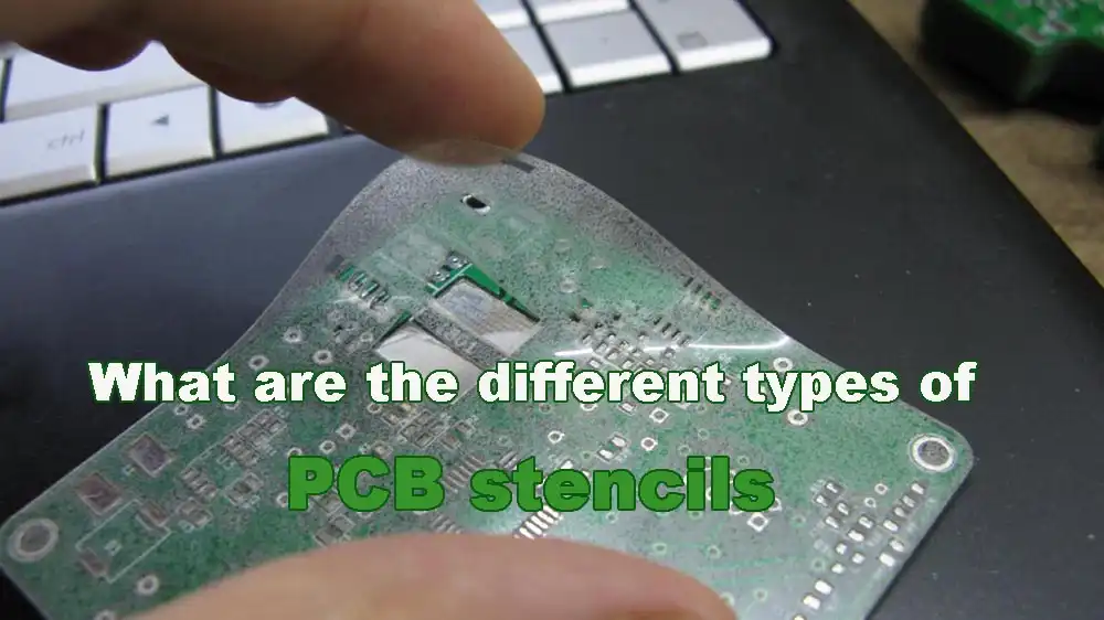
●Laser-cut stencils:
These stencils are created using a laser cutter to cut the pattern into the metal sheet precisely. They offer high accuracy and fine details, making them suitable for small and intricate PCB designs.
●Electroformed stencils:
These stencils are made by electroplating metal onto a plastic or nickel sheet with a pattern etched onto it. They offer high accuracy and fine details, making them suitable for high-density PCB designs.
●Chemical etched stencils:
These stencils are created by coating a metal sheet with a photosensitive material.
The desired pattern is then exposed to ultraviolet light through a photomask and the unexposed areas are chemically etched away. They are suitable for medium to high-volume PCB production.
●Framed stencils:
These stencils are designed with a frame around the cutout pattern. The frame helps to keep the stencil in place during solder paste application and can be reusable.
●Step stencils:
These stencils have multiple levels or steps, allowing different solder paste volumes to be applied to different components on the PCB. They are suitable for PCBs with varying component heights and sizes.
●Hybrid PCB stencils:
These stencils combine laser-cut and chemical etching techniques to create a stencil with the benefits of both methods. The laser cutting technique creates the cutout pattern, while the chemical etching process creates the stencil’s sidewalls. The result is a stencil that offers high accuracy and fine details, better paste release and improved solder joint quality. Hybrid stencils suit PCB designs with fine pitch components, and high-density interconnects.
PCB stencils are a crucial tool in the assembly process of surface-mount technology (SMT) printed circuit boards (PCBs). Solder paste is a sticky mixture of metal particles and flux, which is used to temporarily hold the electronic components in place until the board goes through a reflow soldering process.It helps to apply solder paste to the pads on the board where electronic components will be attached.
The stencil is placed over the PCB and aligned with the solder pads. The solder paste is applied through the openings in the stencil and deposited onto the pads in the exact amount and location needed for the components. The stencil ensures that the paste is applied with high precision, avoiding any risk of bridging or insufficient soldering.
Using a PCB stencil saves time and ensures the accuracy of the solder paste application, improving the efficiency and quality of the SMT assembly process and the whole PCBA process. It is beneficial in mass production of PCBs, where large volumes of identical boards are produced with high consistency and reliability.
PCB stencils are made of thin sheets of metal, such as stainless steel or nickel and holes for pad, which are strong and durable. The metal sheets used for stencils are very thin, with thicknesses ranging from 2 to 6 mils (0.05 to 0.15 mm). The thickness depends on the application and requirements of the PCB design.
The type of metal used for the stencil depends on the specific requirements of the PCB design and the production volume. Stainless steel is the most commonly used material for PCB stencils, as it offers good durability. Other materials, such as nickel and copper, can also be used for stencils in specific applications with advantageous properties.
Some PCB stencils are coated with a special material, such as a non-stick coating or an electroless nickel immersion gold (ENIG) coating. This coating helps to improve paste release and prevent solder paste from sticking to the stencil. These coatings can improve the accuracy and reliability of the SMT assembly process.
1.Prepare the PCB:
Before applying solder paste, the PCB must be cleaned and inspected to ensure it’s free from dust, debris, or contaminants that could impact the solder joint’s quality.
2.Align the stencil:
The stencil should be aligned with the PCB. The alignment fixture or a visual alignment method helps to ensure that the cutout pattern lines up with the solder pads on the PCB.
3.Apply the solder paste:
Once the stencil is in place, solder paste is applied to the stencil’s surface. The paste is spread over the stencil’s surface, filling the cutouts in the pattern.
4.Remove the stencil:
Once the solder paste is applied, the stencil is carefully lifted away from the PCB, leaving the solder paste on the pads. Any excess paste left on the stencil can be cleaned off using a stencil cleaner.
5.Place the components:
The electronic components are then placed onto the pads with the solder paste using a pick-and-place machine or by hand. The solder paste helps to hold the components in place temporarily.
6.Reflow soldering:
Finally, the board is heated in a reflow oven, causing the solder paste to melt and bond the components to the PCB. The result is a finished PCB assembly with high-quality, reliable solder joints.
● Laser cutting:
This method uses a laser to cut a stencil pattern from a metal sheet, such as stainless steel or nickel. Laser cutting is a precise and efficient method that can produce stencils with very fine details and complex patterns.
● Chemical etching:
This method involves coating a metal sheet with a light-sensitive material, exposing it to a patterned mask, and then etching away the unexposed areas with a chemical solution. This process can produce high-quality stencils with good repeatability and accuracy.
● Electroforming:
In this method, a patterned mask is used to electrodeposited metal onto a substrate, building up a thick layer that can be used as a stencil. Electroforming is a precise and repeatable method that can produce stencils with very fine details and complex patterns.
● 3D printing:
Additive manufacturing techniques, such as 3D printing, can also be used to produce stencils for PCBs. This method can be useful for producing unusual shapes or rapid prototyping stencils.
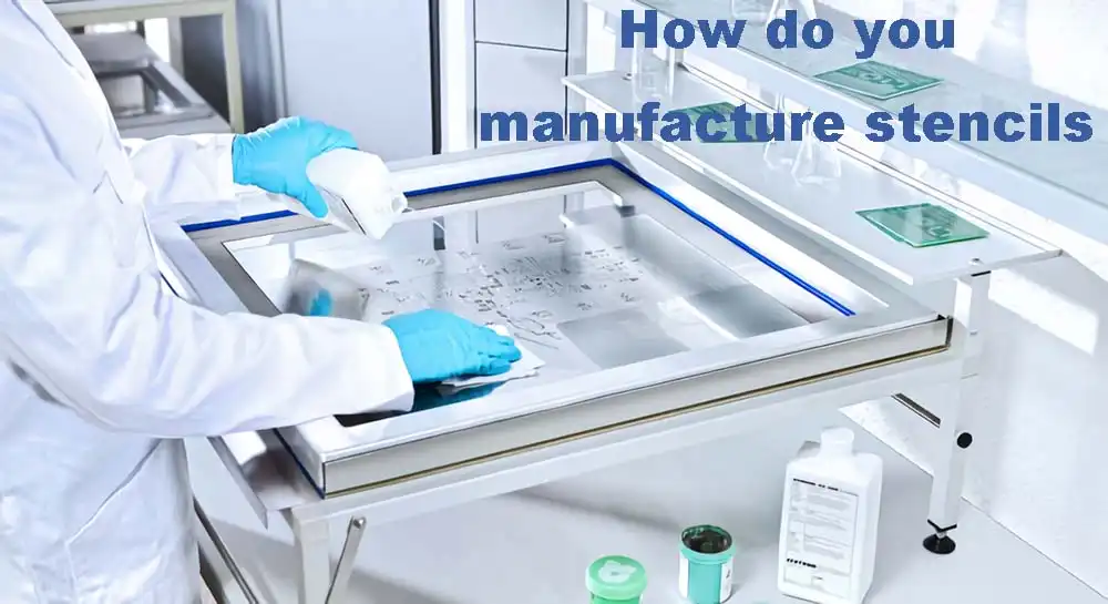
1.Create the design:
The first step in making a stencil is creating a design corresponding to the solder paste pattern needed for the PCB. The design can be created using a computer-aided design (CAD) software or by manually drawing the pattern.
2.Choose the material:
The material used to make the stencil will depend on the specific requirements of the PCB design and the production volume. Common materials used for PCB stencils include stainless steel, nickel, and copper.
3.Choose the manufacturing method:
The method used to manufacture the stencil will depend on the material chosen and the specific requirements of the PCB design. Standard stencil manufacturing methods include laser cutting, chemical etching, and electroforming.
4.Prepare the material:
Depending on the manufacturing method, the material may need to be prepared by cleaning or coating with a light-sensitive material.
5.Apply the design:
The design is applied to the PCB stencil material using a method appropriate for PCB manufacturing and assembly.
6.Clean and inspect:
Once the design is applied, the PCB stencil will be cleaned and inspected for defects or debris that could affect the quality of the solder paste application.
7.Package and distribute:
Finally, the stencil is packaged and distributed to the customer for use in the surface-mount technology (SMT) assembly process.

●Determine the solder paste requirements:
The first step in designing a PCB stencil is determining the solder paste requirements: the type and thickness of solder paste needed, as well as the size and spacing of the pads.
●Create the stencil design:
Once the solder paste requirements are determined, the stencil design can be created. The PCB stencil design is typically done using computer-aided design (CAD) software. The software allows the designer to create a precise pattern corresponding to the solder paste requirements.
●Determine the stencil material and manufacturing method:
The next step is determining the stencil’s material and manufacturing method. The material and method will depend on the specific requirements of the PCB design and the volume of production.
●Add fiducials:
Fiducials are reference marks that help align the stencil and the PCB. Adding fiducials to the stencil design can help ensure the stencil is correctly aligned with the PCB during the surface-mount technology (SMT) assembly process.
●Check for errors:
Before manufacturing the stencil, it’s important to check for errors in the design. This includes checking for any overlaps or gaps in the stencil pattern that could affect the quality of the solder paste application.
●Manufacture the stencil:
Once the design is finalized and checked, the stencil can be manufactured using the chosen material and manufacturing method.
●Clean and inspect the stencil:
After manufacturing, the stencil should be thoroughly cleaned and inspected for any defects or debris that could affect the quality of the solder paste application.
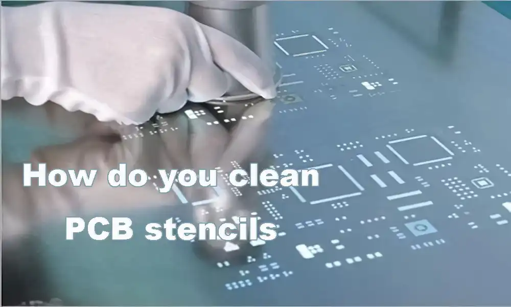
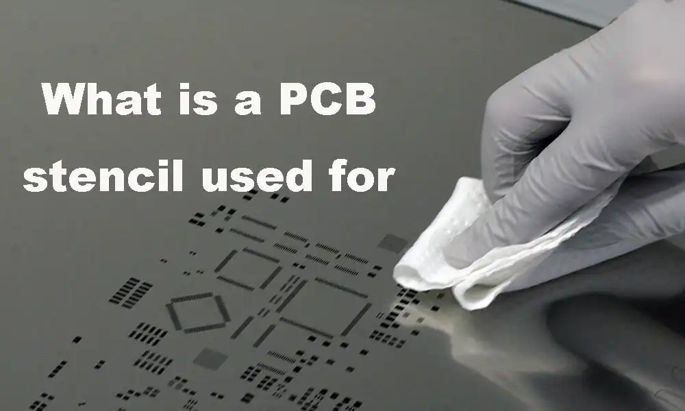
●Remove excess solder paste:
After the PCB stencil is used, excess solder paste should be removed from the stencil. This should be done carefully to avoid damaging the stencil.
●Clean with a solvent:
Once excess solder paste is removed, the stencil should be cleaned with a solvent appropriate for the stencil material. Common solvents used for stencil cleaning include isopropyl alcohol and acetone. The solvent can be applied using a clean, lint-free cloth or sponge.
●Rinse with water:
After cleaning with a solvent, the stencil should be rinsed with water to remove any remaining solvent and debris. The stencil should be rinsed carefully to avoid bending or damaging the stencil.
●Dry the stencil:
After rinsing, the stencil should be dried using compressed air or a clean, lint-free cloth. The stencil should be dried carefully to avoid bending or damaging.
●Inspect for defects:
After cleaning and drying, the stencil should be inspected for defects or debris that could affect the quality of the solder paste application. Any defects or debris should be addressed before the stencil is used again.
The cost of a PCB stencil can vary depending on several factors, such as the size and complexity of the design, the material used, and the manufacturing process. Typically, a simple PCB stencil made of stainless steel or polymer and designed for a small to medium-sized PCB can cost from $50 to $150.
More complex designs, larger stencils, or those made using more advanced manufacturing methods such as electroforming or laser-cutting can cost more, ranging from $200 to $500 or more. Additionally, the stencil cost can vary depending on the quantity ordered, with discounts often offered for larger orders. It’s important to note that these are general estimates, and the actual cost of a PCB stencil can vary based on the specific requirements of the PCB design and the manufacturer used.
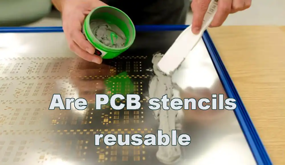
PCB stencils are generally designed to be reusable. However, their lifespan can depend on several factors, such as the quality of the material used, the frequency of use, and the cleaning and storage methods employed.
PCB stencils are typically made of materials such as stainless steel or polymer, which are durable and can withstand repeated use. However, repeated use and cleaning can result in wear and tear, which can affect the quality of the solder paste application. For this reason, stencils may need to be replaced after a certain number of uses or after they become damaged.
To ensure the longevity of a PCB stencil, it’s important to follow proper cleaning and storage procedures after each use, most important of which, removing excess solder paste, cleaning the stencil with an appropriate solvent, rinsing with water, and drying thoroughly before storage. Stencils should also be stored in a dry, cool place to prevent rusting or other damage.
Overall, with proper care and maintenance, PCB stencils can be reused many times, which can help reduce the overall cost of the SMT assembly process.