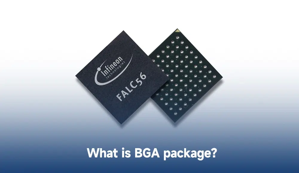
The packaging technology known as BGA(Ball Grid Array) has caused a paradigm shift in the electronics manufacturing industry by introducing a groundbreaking technique that boasts unrivaled precision and efficiency. Its widespread adoption across different sectors, such as telecommunications, consumer electronics, defense, and aerospace, is a testament to its exceptional benefits. BGA technology stands out from other packaging techniques due to its unparalleled advantages, making it an increasingly popular choice for state-of-the-art electronic devices.
In this article, we will explore the features, types, and benefits of it, as well as the steps involved in soldering BGA to a PCB, common defects, and inspection methods.

The Ball Grid Array (BGA) packaging method has ushered in a new era of integrated circuits packaging in the world of electronics by replacing pins with a matrix of solder balls that sit at the base of the package, triggering a revolution in the field.
This package type is designed to be surface-mounted, which means it can be mounted on the surface of a printed circuit board (PCB). BGA packages have become increasingly popular due to their compact size and high pin count, making them ideal for use in devices with limited space.
At the heart of BGA lies a defining characteristic – an exceptional pin count that facilitates the unification of intricate circuits and functionalities within a solitary package, a quality that has positioned it as a standout in the world of electronics.
BGA packages are also known for their low profile, which reduces the overall size of the PCB. This feature is particularly useful in the design of small electronic devices, such as smartphones and tablets. In addition, BGA packages offer better electrical performance and reliability compared to other packaging technologies.

BGA packages come in diverse variations, each crafted to fulfill distinct application demands, providing a flexible and versatile option for electronics manufacturers. The most common types include ceramic, plastic, and tape-based BGA.

The BGA package is a type of integrated circuit packaging that has an array of tiny solder balls on the bottom. The solder balls in BGA packages act as a conduit, enabling a seamless electrical link between the Integrated Circuit (IC) and the Printed Circuit Board (PCB), thereby ensuring optimal functionality.
BGA packages are available in different sizes and pin counts, and they are designed to be surface-mounted on the PCB. The BGA package provides a compact and reliable solution for electronic devices with high pin counts.

BGA, PGA, and LGA packaging technologies are the cornerstones of modern electronics manufacturing, embodying the pinnacle of engineering excellence and offering unique benefits to empower the advancement of technology. BGA offers several advantages over PGA and LGA, including higher pin counts, better electrical performance, and improved reliability.
BGA also allows for smaller and more compact designs, making it a popular choice for modern electronic devices. Despite its benefits, BGA packages have a few drawbacks that include a steep price point and challenges in reworking or repairing, issues that manufacturers must consider while adopting this innovative technology.

Soldering a Ball Grid Array (BGA) to a Printed Circuit Board (PCB) is an intricate process that demands skill, patience, and precision. The complexity of this technique requires specialized tools and techniques to ensure that the soldering process is successful. Below is a step-by-step guide on how to solder a BGA to a PCB.
1.PCB preparation: Before the BGA is soldered to the PCB, it is essential to prepare the PCB first. This involves cleaning the PCB surface to remove any impurities or debris that may affect the soldering process. The next step is applying solder paste to the BGA pads. To ensure precise placement and uniform coverage of the pads, a stencil is used to apply the solder paste.
2.BGA placement: After the PCB has been prepared, the BGA is carefully positioned on the PCB, making sure that all the balls align with the corresponding pads. The process requires a steady hand, attention to detail, and a good eye for precision.
3.Reflow soldering: The next step in the process is reflow soldering. Reflow soldering is a heating process that melts the solder paste and forms a permanent connection between the BGA and the PCB. This process is usually done in a reflow oven that heats the PCB and the BGA to a specific temperature profile. The temperature profile is critical as it ensures that the solder paste melts evenly and forms strong bonds.
4.Inspection: Once the BGA is soldered, it is important to inspect the solder joints to ensure that they are correctly formed and there are no defects. Visual inspection or automated inspection tools can be used to ensure that the joints are strong and that there are no issues that may affect the operation of the circuit.
To achieve a dependable connection when soldering a BGA package, specialized equipment, and a distinctive process are necessary, and multiple considerations must be factored in to guarantee optimal results. These factors include:
●Solder paste: The type and quality of the solder paste used in the process can affect the quality of the connection. It is important to choose a high-quality paste that is compatible with the BGA package and PCB.
●Temperature profile: The temperature profile of the reflow process is critical to ensure that the solder paste melts and reflows correctly without damaging the components or PCB.
●Alignment: Proper alignment of the BGA package with the PCB is crucial to ensure a reliable connection. The tiniest misalignment in BGA soldering can lead to detrimental outcomes, including weak connections, vacancies, or even cracks in the solder joint, making precision a critical aspect of the process.
●Inspection and testing: Inspection and testing should be performed after the BGA is soldered to the PCB to ensure that the connections are free from defects and meet the required specifications.

BGA soldering is often a complex undertaking, with multiple potential pitfalls that could result in common defects during the process, making it crucial for BGA packaging substrate suppliers to take great care and employ best practices. These defects include:
●Solder ball fractures: Solder ball fractures can occur due to excessive stress or strain during the reflow process. To prevent this, it is important to ensure that the temperature profile is appropriate and that the BGA package is properly aligned with the PCB.
●Voids: Voids are air pockets that can form in the solder joint, reducing the quality of the connection. To prevent voids, it is important to use a high-quality solder paste and ensure that the reflow process is carried out correctly.
●Insufficient solder paste: Insufficient solder paste can result in poor connections or open circuits. To prevent this, it is important to apply a sufficient amount of solder paste to the PCB pad.
●Bridging: Bridging occurs when two or more solder balls fuse together, creating a short circuit. To prevent bridging, it is important to ensure that the temperature profile is appropriate and that the BGA package is properly aligned with the PCB.
To solve these defects, rework or repair may be necessary. Reworking or repairing a BGA package can be challenging and requires specialized equipment and skills.
BGA soldering requires precise alignment and reliable connections, which can be challenging to achieve. The importance of thorough inspection in BGA soldering cannot be overstated, as it is essential to ensure that the connections meet the required specifications and are entirely free of defects.
Manufacturers have access to several inspection techniques, each with its unique advantages, to guarantee the integrity of BGA connections, including:
1.X-ray inspection: When it comes to inspecting BGA connections, X-ray inspection is a favored technique for its ability to provide a high resolution. It allows for a non-destructive inspection of the connection, ensuring that there are no voids, cracks, or other defects in the solder joint. X-ray inspection can also detect misaligned or missing solder balls.
2.Optical inspection: Optical inspection involves visually inspecting the BGA connections under a microscope. This method can detect defects such as poor alignment, insufficient solder paste, and solder ball fractures. Optical inspection is also useful for inspecting the PCB pads and vias to ensure they are free from defects.
3.CT scanning: CT scanning is a three-dimensional X-ray imaging technique that can provide more detailed information about the BGA connections. CT scanning can detect voids, fractures, and other defects that may not be visible with traditional X-ray inspection.
4.Acoustic microscopy: Acoustic microscopy uses high-frequency sound waves to inspect the BGA connections. This method can detect voids, cracks, and other defects that may not be visible with X-ray inspection or optical inspection.
5.Electrical testing: Electrical testing involves measuring the electrical characteristics of the BGA connections to ensure that they meet the required specifications. This method can detect defects such as open circuits, short circuits, and excessive resistance.
6.Cross-sectional analysis: Cross-sectional analysis is a microscopic inspection technique used to assess the quality and structure of BGA connections by slicing and polishing a segment of the solder joint. This method offers a detailed examination that can reveal vital information about the BGA’s performance, reliability, and structural integrity.
7.Shear testing: By exerting a precise amount of force on the BGA connection, shear testing provides a reliable and effective way to evaluate the joint’s strength and dependability. Manufacturers can detect flaws such as brittle or weak solder joints, allowing them to rectify these defects and ensure the BGA’s quality and longevity.
Each of these inspection methods has its advantages and limitations, and the choice of method will depend on the specific requirements of the application. Combining multiple inspection methods can provide a more comprehensive analysis of the BGA connections and ensure their reliability in electronic manufacturing.