blogs
Qtech Technology Co., Ltd
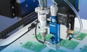
SMT / DIP / PCB assembly /
Testing / BGA reworking
QUOTE
close
SMT / DIP / PCB assembly /
Testing / BGA reworking

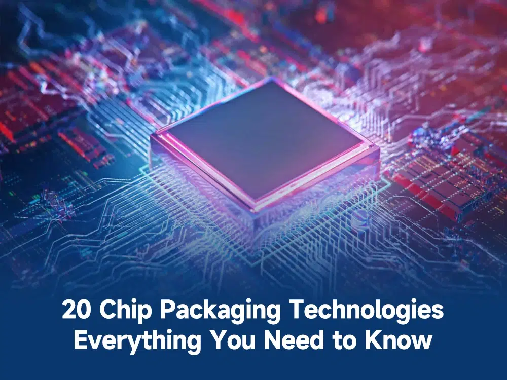
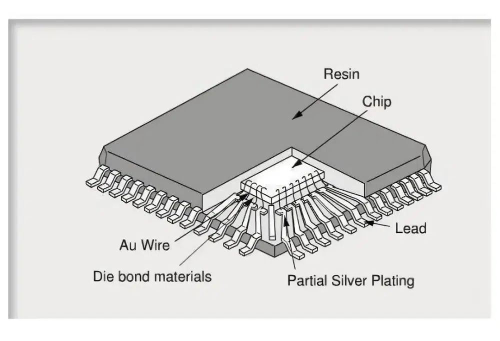
The shell used to install the semiconductor integrated circuit chip plays the role of placing, fixing, sealing, protecting the chip and enhancing the electrothermal performance. Therefore, chip packaging plays an important role for CPUs and other LSI integrated circuits. The emergence of a new generation of CPU is often accompanied by the use of new packaging. Chip packaging technology has gone through several generations of changes, from DIP, QFP, PGA, BGA, to CSP and then to MCM, and the technical indicators are more advanced from generation to generation. This article summarizes 20 chip packaging technologies for you.
| Package Type | Fuall Name | Time |
|---|---|---|
| DIP | Dual In-line Package | Before the 1980s |
| SOP | Small Out-line Package | 1980s |
| QFP | Quad Flat Package | 1995-1997 |
| TAB | Tape Automated Bonding | 1995-1997 |
| COB | Chip on Board | 1996-1998 |
| CSP | Chip Scale Package | 1998-2000 |
| FC | Flip Chip | 1999-2001 |
| MCM/CSP/SIP… | Multi-Chip Model | 2000-present |
| WLCSP/TSV… | Wafer Level Chip Scale Packaging | 2000-present |
The TO package is called a transistor outline package, which is a long-standing form of packaging.
This type of package usually uses the heat dissipation pad on the back as the drain, which is directly soldered to the PCB, so that it can dissipate heat through the PCB while ensuring a large output current. This is a very old form of packaging.
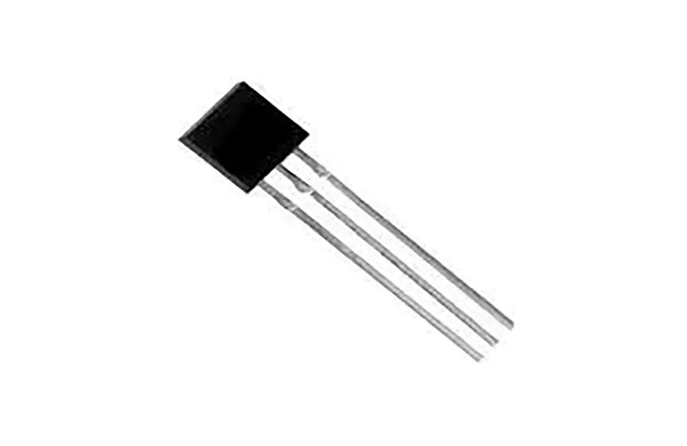
DIP, Dual In-line Package, can be seen in many small and medium-sized integrated circuits.
The DIP package is suitable for perforation soldering on the PCB board, but it can be seen from the picture that it has a large volume and a large pin spacing.
According to the packaging material, it can be divided into plastic and ceramic packages.
SOP can also be called SOIC, Small Out-line Integrated Circuit, which is a reduced version of DIP package. In fact, it reduces the lead spacing and miniaturizes the package on the basis of DIP.
The standards of SOP packaging include SOP-8, SOP-16, SOP-20, SOP-28, etc., and the numbers indicate the number of pins. According to the materials, there are also two types: plastic and ceramic packages, specifically TSOP (thin small outline package), VSOP (very small outline package), SSOP (shrunk SOP), and TSSOP (thin shrunk SOP).
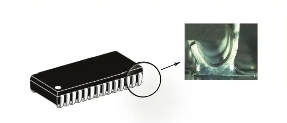
The BIOS on the early computer motherboards all adopt this package form, which has a small assembly area, high lead strength, and is not easy to deform. Multiple leads ensure good coplanarity for better consistency of solder joints. However, the pins are J-shaped and bent to the bottom of the device, making it difficult to overhaul.
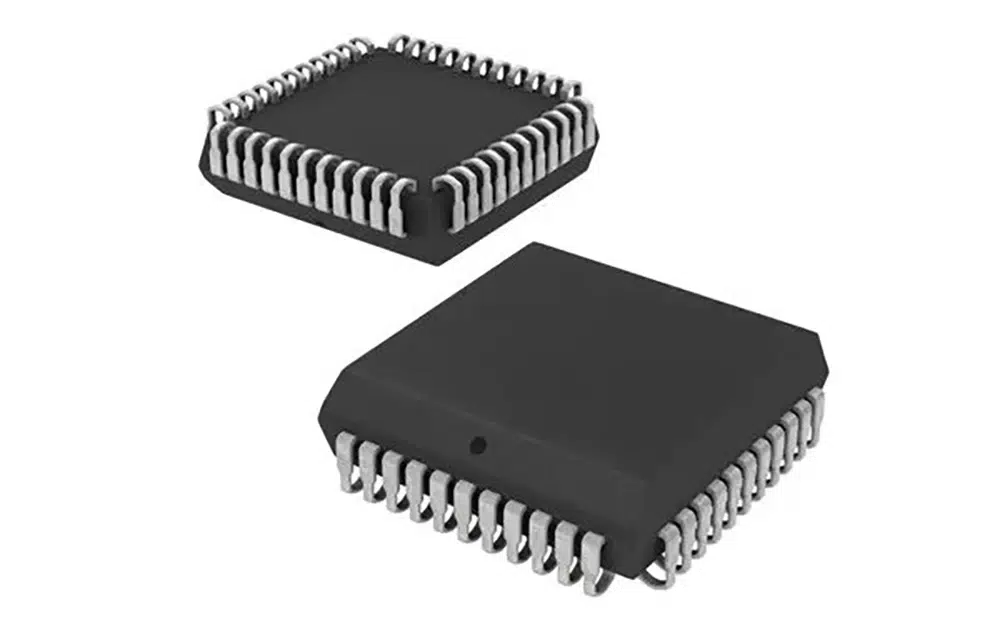
QFP, Quad Flat Package.
The BIOS on the early computer motherboards all adopt this package form, which has a small assembly area, high lead strength, and is not easy to deform. Multiple leads ensure good coplanarity for better consistency of solder joints. However, the pins are J-shaped and bent to the bottom of the device, making it difficult to overhaul.
QFP, Quad Flat Package.
This type of package structure can be seen on many PCB boards and is one of the surface mount packages. According to the material, it is divided into three types: ceramics, metals and plastics. Most of QFP refers to plastic packaging, which is also the most common in large-scale multi-pin integrated circuit packaging. The pitch of the pins is 1.0mm, 0.8mm, 0.65mm, 0.5mm, 0.4mm, 0.3mm, etc., and the number of pins in the 0.65mm specification can reach 304.
QFN, Quad Flat No-lead, also known as LCC.
In the QFN package, there is a large-area exposed pad at the center of the bottom of the chip package, and the periphery of the package around the large pad is surrounded by I/O pins. The short lead makes its self-inductance coefficient and lead resistance in the package very low, so it has better electrical performance. At the same time, it can also dissipate heat through the exposed lead frame pads, and directly conduct heat on the PCB board.
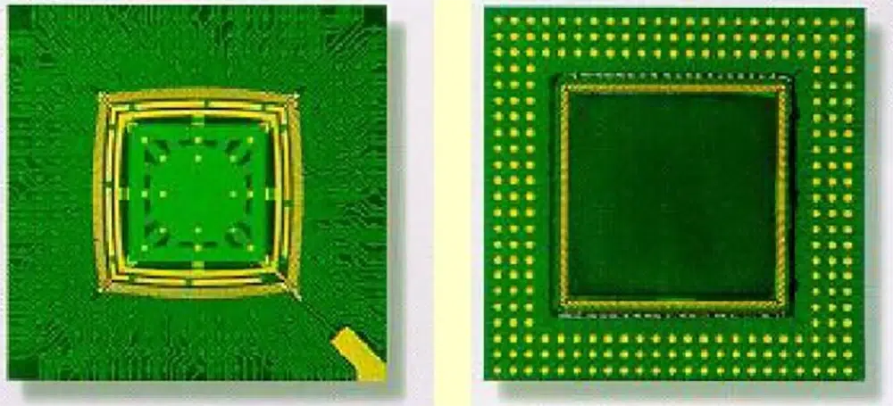
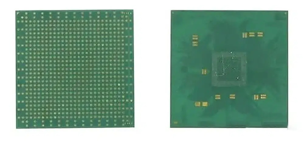
BGA, Ball Grid Array. With the development of integrated circuits, the scale of the chip is getting bigger and bigger, the number of pins is getting more and more, the interface rate of the chip is constantly increasing, and the requirement for the inductance introduced by the package is getting smaller and smaller. The use of WB (Wire Bonding, wire bonding method) encountered a bottleneck, and the emergence of the BGA method solved this problem.
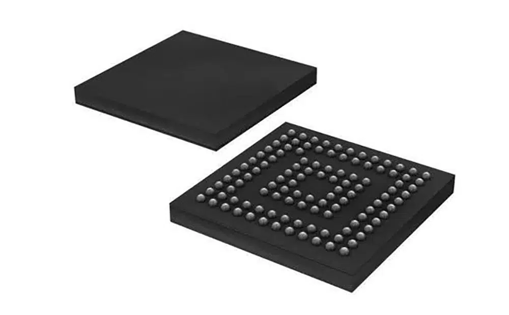
BGA has the following characteristics:
The external difference of BGA package is not very big, mainly the difference between the connection methods inside the chip, so the types of BGA are also various, and the typical packages are as follows:
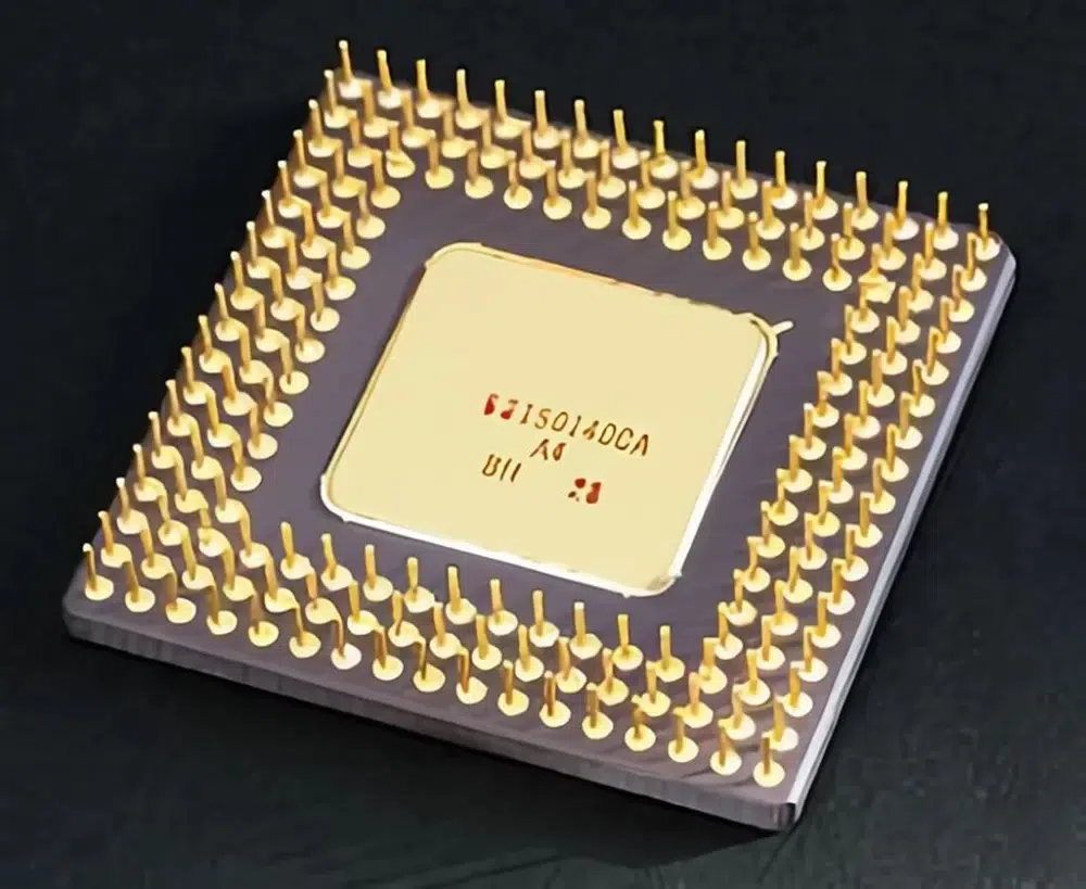
PGA, Pin Grid Array, this packaging method has multiple target-shaped pins on the outside of the package. Each pin is arranged at a certain distance along the periphery of the chip. According to the number of pins, it can be surrounded by 2-5 circles. When installing, insert the chip into the dedicated PGA socket.
LGA, Land Grid Array, the pad is made on the ground of the substrate, and the surface mount method is used for installation.
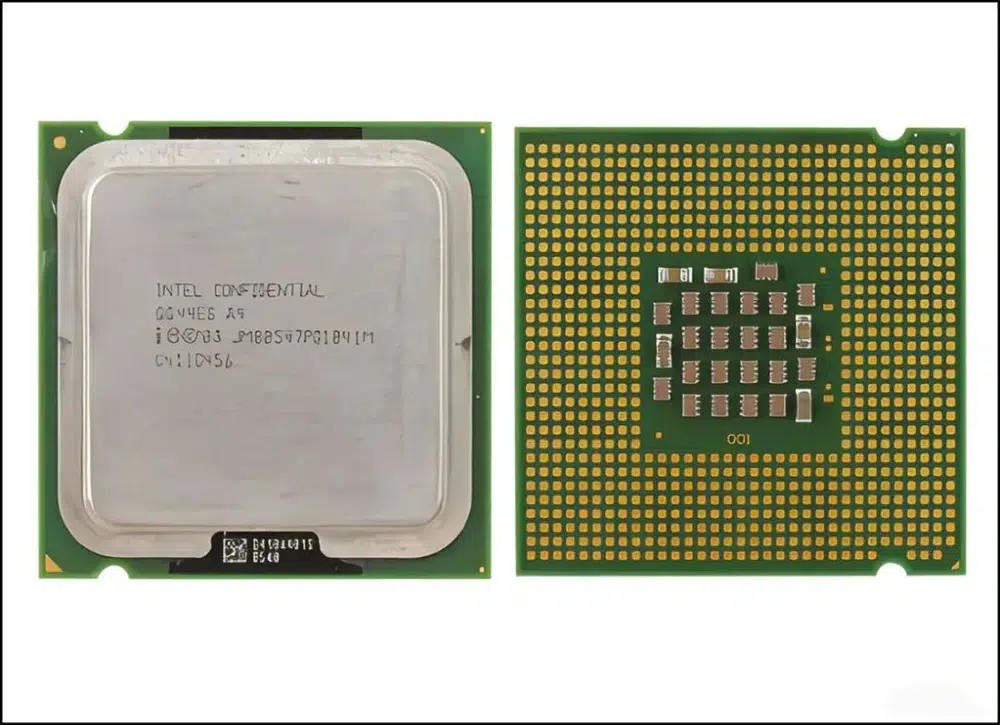
LGA has light weight, small size, good mechanical and thermal performance, and it can accommodate more I/O pins than QFP. The inductance effect of LGA is further reduced, so it can be used in higher frequency band and higher speed chips.
TBGA, Tape Ball Grid Array, is the evolution of TAB technology.
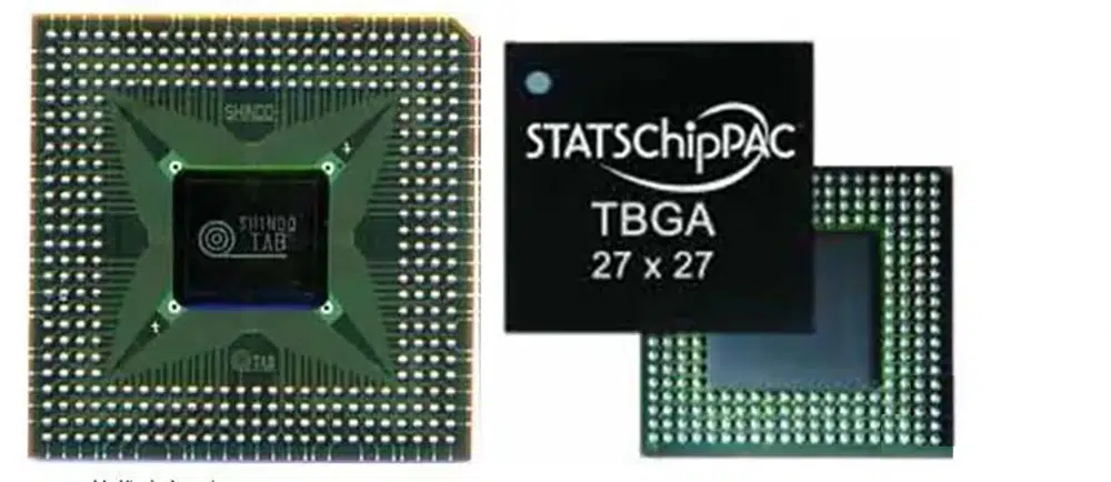
The carrier of TBGA can be divided into copper or polyimide or copper bimetal carrier tape, and the chip and the carrier are interconnected. Through holes are used to connect the upper and lower surfaces, and soldering technology is used to connect the surface pads, and then an array of solder balls is formed on the bottom pads with windows. Solder ball spacing is 1.0mm, 1.27mm, 1.5mm and so on.
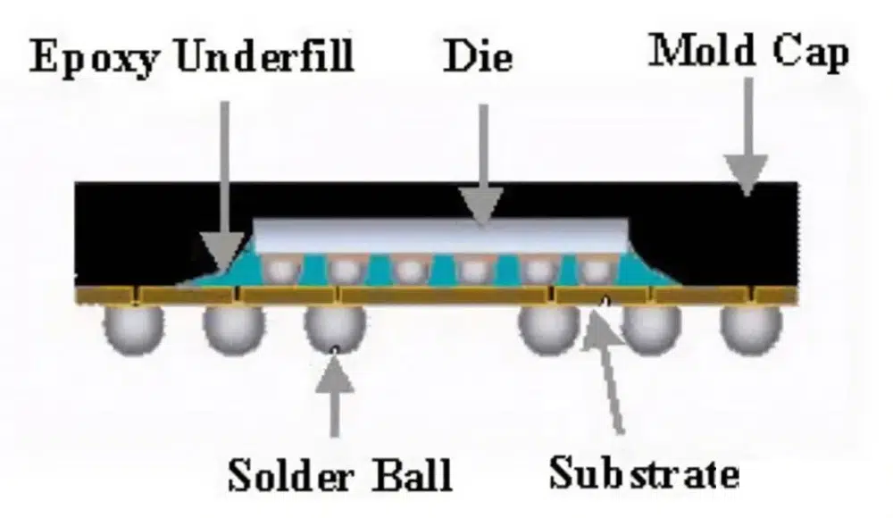
PBGA, Plastic Ball Grid Array. As the name suggests, its packaging material is plastic. Use BT resin or glass cloth as the substrate, and then use epoxy molding compound as the sealing material. The solder balls are eutectic solder 63Sn37Pb, quasi-eutectic solder 62Sn36Pb2Ag or lead-free solder.
The structure of some PBGAs is a cavity structure, which can be divided into two types: upward and downward according to the orientation of the cavity. The structure with a cavity is mainly to increase its heat dissipation capacity in the future, that is, EBGA, sometimes called CPBGA.
Advantages of PBGAs:
CSP, also known as FBGA: Fine Pitch BGA, is based on the evolution of PBGA. The emergence of CSP has further reduced the size of the packaged chip. The side length of the packaged chip is <1.2 times the chip die, <1.4 times the packaging area.
In addition, CSP can accommodate more I/O pins under the same package area. The reduced area reduces the path of signal transmission and greatly reduces the delay of signal transmission.
CSP package is divided into:
WLCSP, Wafer Level Wafer Level Chip Scale Package. The traditional chip packaging is to cut the chip from the wafer and then package it. The area of the chip after packaging is at least 20% larger than that of the original die. In WLCSP technology, the chips on the entire wafer are first packaged and tested and then cut into individual ICs, so the packaged chip area is basically equal to the size of the original bare chip.
FC-PBGA, Flip-Chip Plastic Ball Grid Array. The chip uses the Bump connection method and is connected with a multi-layer substrate. It has the characteristics of a high number of pins, easy suppression of high-frequency noise, and high-speed transmission. The size of FC-PBGA can be more than 50mm×50mm, and the number of pins is more than 2500.
MCM, multi-chip module package, a module composed of two or more bare chips and other components assembled on a substrate, and then packaged together.
The substrate can be PCB, thick-film ceramics, thin-film ceramics, or silicon wafers with interconnected wiring. The entire MCM can be packaged on the substrate, or the substrate can be packaged inside the package. According to the process method and the substrate material used, it can be divided into the following three types:
SIP, System in Package, according to the definition of ITRS, SIP is to assemble multiple active electronic components with different functions, optional passive devices, and other devices such as MEMS or optical devices in a package to achieve certain functions. Simply put, several independent chips + some separate components are packaged together in one package to form a system or subsystem module.
The simpler SIP can be integrated on the substrate by several bare chips plus some discrete components.
SOC, System on Chip, integrates system functions in a single chip, and packages the chip to form a system-level functional device. SOC implements chips with multiple functions in one chip, which further improves the integration level.
Although the advantages of SOC are obvious, it also faces some technical limitations. It is extremely difficult to integrate digital, analog, radio frequency, MEMS, etc. on the same chip, the processing technology is limited, and heat dissipation cannot be solved. In addition, complex system interconnection, design errors, product iteration delays, low yield and chip manufacturing costs have further increased the risk of implementation, and it is difficult to reduce costs.
PIP, Package in Package, it is actually a form of stacked package, and a package is packaged with another chip or passive device to form a new package. The outline height is high, and the standard SMT circuit board assembly process can be adopted, then the assembly cost of a single device is low. However, comprehensive testing cannot be realized after packaging, and the yield rate cannot be guaranteed.
POP, Package on Package, is also a form of stacked package, and components are placed on top of the bottom components. It is suitable for stacking complex logic devices and memory devices (common in stacked memories), which require faster digital signal processing and larger storage capacity, such as baseband processors. High-density or combination memory devices such as DRAM or Flash can be stacked in the top package.
POP solves the problem that each component in PIP cannot be tested. A single section can be tested separately, and the yield rate is higher. Devices can be freely combined to facilitate product design and upgrades.